|
|
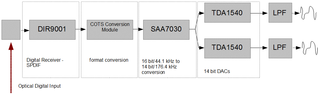
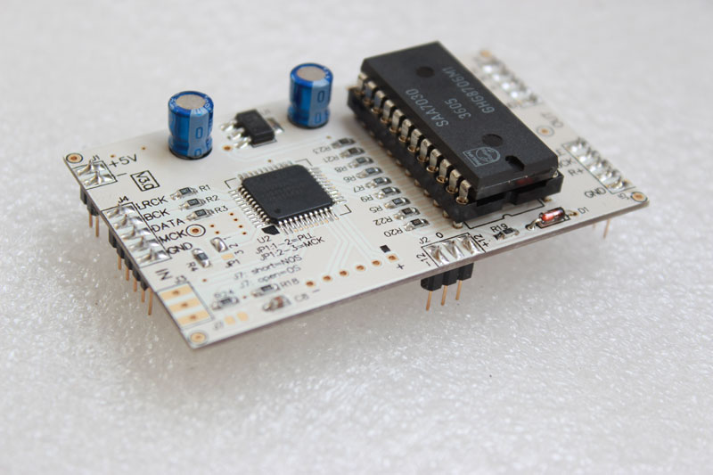
TDA1540 DAC updated 2022/03/22 10:30 The primary goal of this project is to interface a Philips SAA7030 digital filter to a Burr Brown DIR9001 digital audio interface. The SAA7030 was never designed to interface to anything except the SAA7000 interpolation and muting circuit in a CD player. A Xilinx CPLD (tried a dsPIC33) is therefore used to emulate the output signals of an SAA7000 and convert audio samples from 2s complement to offset binary format. This project will use the Philips TDA1540 DAC which was also used in the very first CD player Philips sold in 1983, the gorgeous CD100. This project was formerly called "Goldilocks" because I wanted to use two Burr Brown DACs. I've decided to use the lessons learned from this project to make another version with Burr Brown DACs later on.
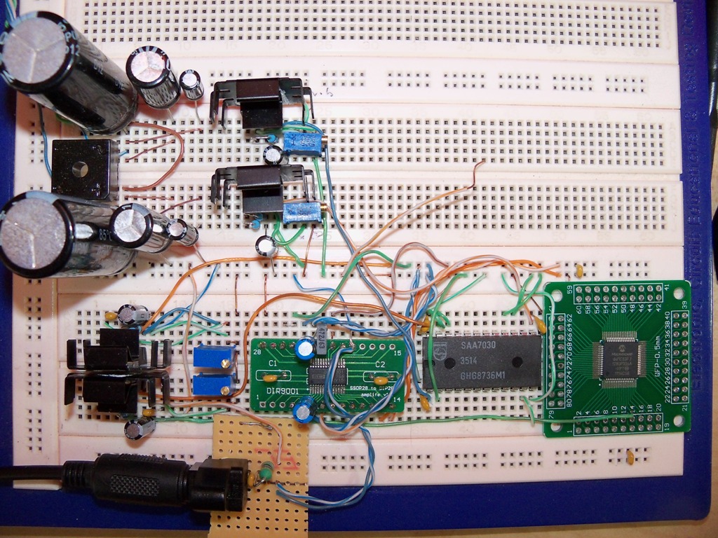
SPECIFICATIONS Twin Philips TDA1540P 14 bit DACs Analog output stage from Philips CD100 Philips SAA7030 4 x oversampling digital filter with noise shaping Burr-Brown DIR9001 Digital Audio Receiver Optical Digital Interface Commercial off-the-shelf conversion module Development Blog 10 January 2012
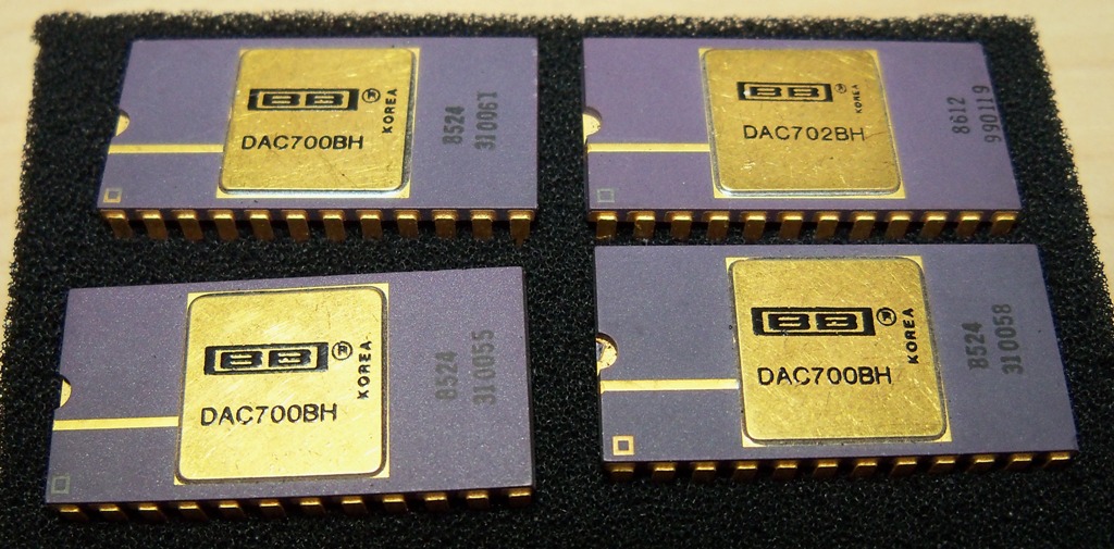
The Burr Brown DAC700BH and 702BH chips. The Gold in Goldilocks I did much research the last week and decided to use a dsPIC33 between the DIR9001 and SAA7030. The SAA7030 requires a multitude of bizarre clock/strobe pulses. It also requires data in offset binary instead of 2s complement, which requires a conversion. This conversion is performed by the dsPIC33. The PIC can also provide the correct clock pulses and strobe pulses to the SAA7030. The dsPIC replaces at least 12 discrete logic chips. I also have two TDA1540 14 bit DACs I'd like to try out. The TDA1540 is of course the DACs originally used together with the SAA7030 in the first Philips CD player the CD100 in 1982. 11 January 2012
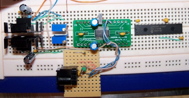
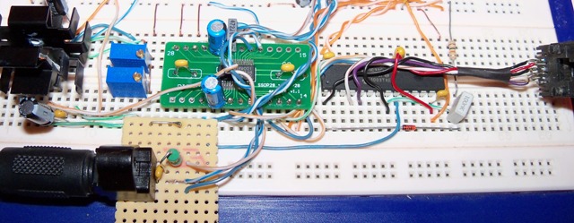
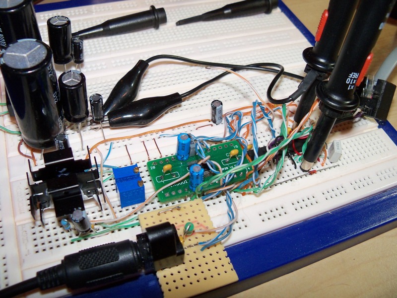
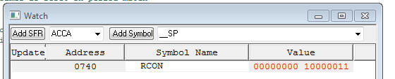
DIR9001 in the middle with dsPIC33 to the right, optical interface is below on veroboard I added the TOSLINK interface using a TORX177 module. The dsPIC33 has a built-in audio Delta-Sigma DAC. Once samples have been converted from 2s compliment to offset binary, the converted samples will be sent to the dsPICs onboard DAC so I can confirm they're correct. At the same time the samples will be streamed out to the SAA7030 via the two SPI interfaces. 14 January 2012
I tested the SPDIF decoder. Everything works. I connected up the dsPIC33. Now I have to start writing some software to convert the samples from the DIR9001 to the correct format for the SAA7030 digital filter.
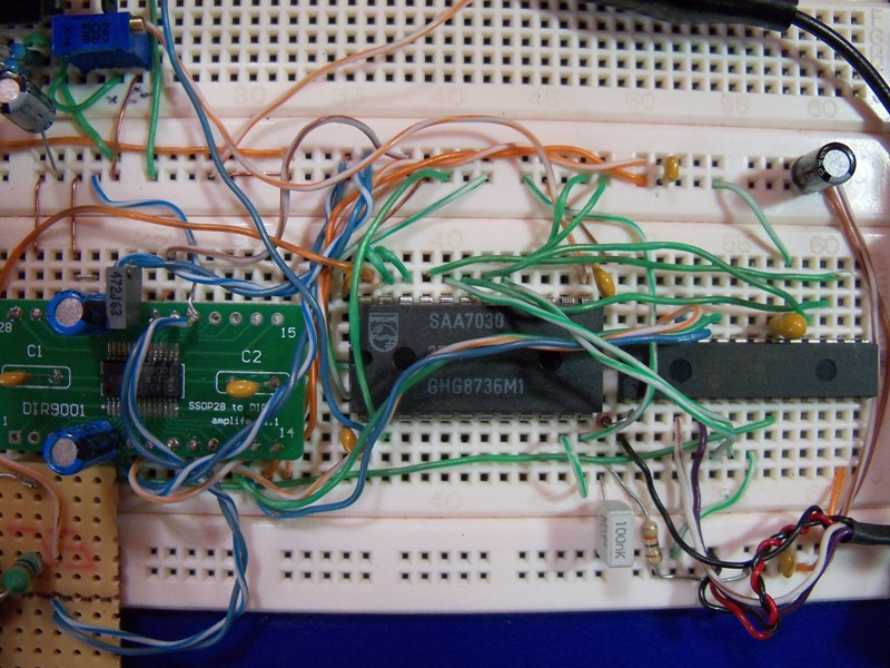
The output from the DIR9001, showing left channel sample followed by right channel sample (top) 15 January 2012 Installed MPLAB IDE and confirmed comms to the dsPIC. 19 January 2012 Started writing control software. Researched how I'm
going to use the Output Compare, SPI and Timer modules. 21 January 2012
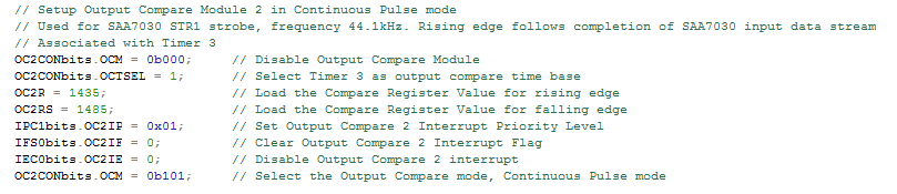
Got the dsPIC code working to generate the 4.2336MHz clock for
the SAA7030 from the DIR9001 system clock (16.9344 MHz). I'm using Timer2 and
the OC1 module. I'm just going to re-check the frequencies.
CODE
22 January 2012
Confirmed correct CLOX frequency is being produced by the dsPIC,
4.2336MHz. CLOX and STR1 need to be synchronous. Right now there's a small
(~40ns) difference between the two due to the fact that I cannot activate Timer
2 and 3 at exactly the same time. I'm planning to just add a small delay to the
one using a 74HCT04 so that the two signals align better.
CODE
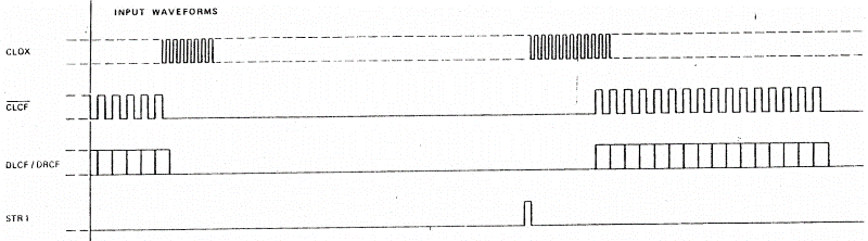
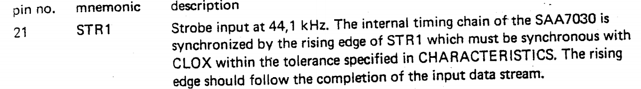
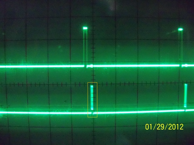
(Above) What the SAA7030 expect. See CLOX and STR1.
CLCF and DLCF/DRCF will come from the SPI interface
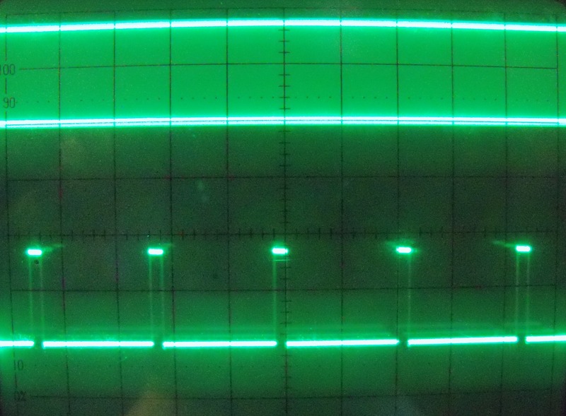
(Above) CLOX at the top (4.2336MHZ) and STR1 at the
bottom (44.1kHz)
23 January 2012
I wrote some
alternative code in
an attempt to synchronize Timer2 and 3. The idea was to use the CLOX output to
clock timer 3 which in turn controls the OC module for STR1. The final effect
was the same as the earlier code that just
ran both off of the internal timebase. So I kept the earlier code. It's simpler.
I implemented a 74HCT04 and sent CLOX through it 6 times. The
result is that STR1 (high-low) and CLOX is now aligned as close as is possible. Todays
CODE.
Without the delay, the low-high transition of STR1 is aligned
with the low-high edge of CLOX. It looks like the edge of STR1 can be off by up
to 55ns, as shown below from SAA7030 datasheet.
(Above) CLOX at the top and STR1 at the
bottom, no delay. Scope sweep triggers on rising edge of STR1
24 January 2012
It occurred to me that I was being stupid trying to add an
external delay to STR1 to align it with CLOX. I made some
sketches and realised that adjusting PRx for the
timer sets the period or frequency while adjusting OCxR and OCxRS for the OC
modules will adjust their relative phases. Timers 2 and 3 are off by one
instruction cycle time due to the fact they I cannot enable them at exactly the
same time. If you adjust for that in your setting of OCxR and OCxRS their
shouldn't be a phase difference between CLOX and STR1. The question to ask
is:"At what count is T3 when T2 resets after its' period rolls over the first
time?". That'll be your first OC trigger point. I'll test it out later.
28 January 2012
Started the code for the Data Converter Interface as well as the
two SPI modules, one per output channel. CODE
29 January 2012
I added code for the SPI, DCI and port pins, but then the PIC
started acting weird. Sooo, I rolled back the code to an earlier version and
started fresh. I needed to confirm that the Timer3 interrupt that triggers
whenever the timer resets does not disrupt the OC1 module output (CLOX). So I
devised an experiment. Below is a screenshot of this
CODE. At the top is the output of the
Output Compare module producing CLOX at 4.2336MHz. Below CLOX is an
on-off-on-off waveform being produced inside the Timer3 interrupt. You can see
that both waveforms are continuous. Neither one is affecting the other. This
means that output compare modules carry on happily regardless of interrupts and
what the processor is doing. I thought as much, but when the previous code
started acting weird, I just had to convince myself.
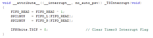
The Timer3 interrupt triggers after STR1 (OC2) goes low. This is
where the SPI left and right sample writes to the SAA7030 will be triggered.
This is the CODE that acted weird.
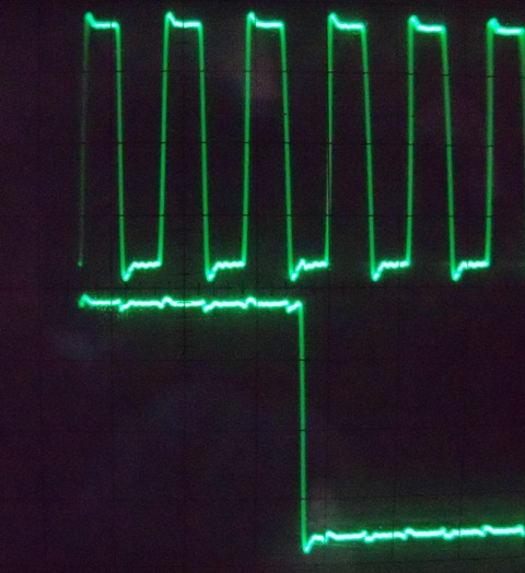
Top waveform is CLOX (OC1). Lower waveform is produced
in Timer3 interrupt
32 Instructions fit into the highlighted waveform. The
highlighted waveform is produced during the Timer3 interrupt. STR1 is the top
waveform.
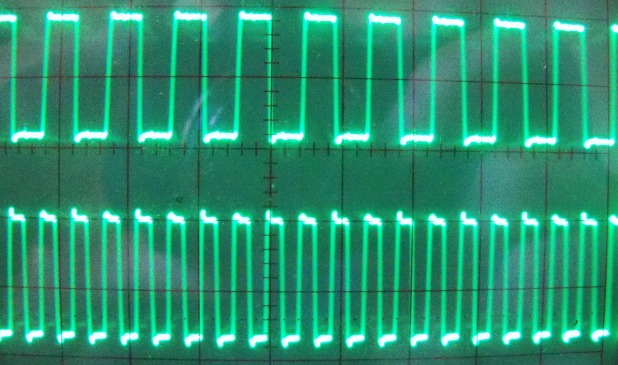
19 February 2012
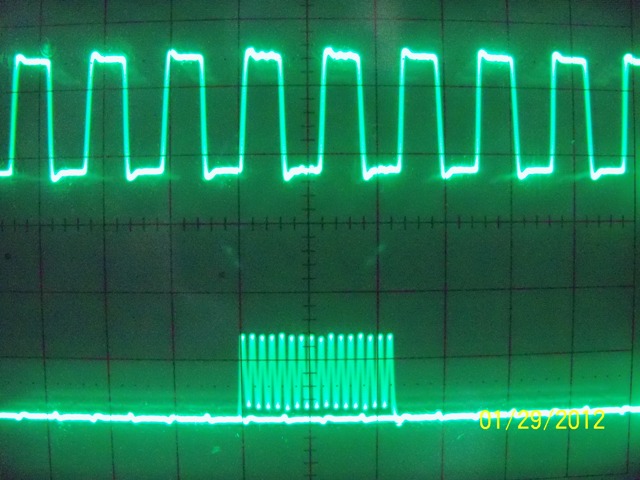
The SPI interfaces are working now. They read out dummy data
still. If you look below, I now have CLOX, CLCF (SPI clock out), DLCF and DRCF
(SPI1 and 2 data out) as well as STR1. That takes care of the control signals.
The rest is fine tuning. Here's todays' code.
The last thing is to activate the DCI (Data Converter Interface)
and read audio samples in from the DIR9001 for conversion and retransmission out
on the SPI interfaces to the SAA7030. Compare the datasheet diagrams with the
on-screen oscilloscope photos.
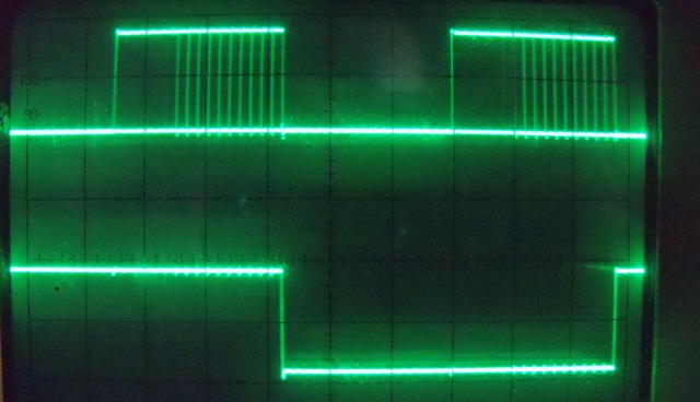
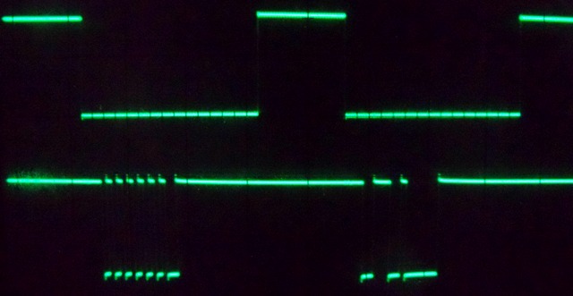
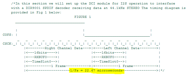
Input signals required by the SAA7030 digital filter
(top)
Top is CLCF at 2.1168MHz, bottom is CLOX at 4.2336 MHz
Top is CLCF data clock at 2.1168MHz in bursts, bottom
is STR1 at 44.1kHz
Top is DLCF dummy data, bottom is STR1 at 44.1kHz
26 February 2012
I am having severe problems going further. Simulated code that
works perfectly refuses to run correctly on the dsPIC. Standard C data
structures and arrays refuse to work as expected. Adding or removing a simple
command such as FIFO_R = 0, makes the difference between normal operation
and the PIC not running at all! The behaviour is so strange that I re-installed
the compiler. Next I'm going to try a different chip. I used known working code
from my PCM-X2, even this behave strangely. I usually find faults, but I have
never struggled like this. There is no cause and effect.
3 March 2012
After trying many different possible solutions I have decided to
split the functionality across two dsPICs to facilitate debugging. Doing so
allowed me to make progress once again. Functions are now split between
generating STR1 and CLOX on the one dsPIC and performing DCI data reads, sample
conversion and SPI write on the other dsPIC. The two chips are synchronised via
STR1. Goldilocks20120303-2CONTROL.zip
Goldilocks20120303_LOGIC_DATA.zip
STR1 (top) with alternating dummy SPI data (bottom). I
could not get this to work before
23 March 2012
Often when you try to eliminate one problem, you create two more.
Closer scrutiny with a digital scope has revealed that there is quite a bit of
jitter between STR1/CLOX and the SPI data clock. These two signals come from
different chips. The sync is therefore not perfect. I'm concerned that this
jitter will come back to bite me later. Sooo, I'm going back to ONE chip. The
two chips were useful for checking code, but from an engineering standpoint it's
messy.
Speaking of messy
24 March 2012
10:00 - OK. I'm getting time to work on this again. Things are slowing
down at the university towards easter break. I've combined the code again. The
SPI modules work as well as the STR1 and CLOX. Unfortunately the SPI is only
managing to spit out dummy data. As soon as I declare out a piece of code that
fills an array with dummy data the processor doesn't run. Some sort of memory
trap? I'll have to investigate. I'm beginning to think that using a PAL or FPGA
might have been easier...? Then again the easy path is not always the best path.
15:45 - I managed to
get everything working on one chip. I do still have one small problem with the
one SPI interface. The two doesn't seem to like running together. I have
isolated the problem down to a single instruction that will cause the chip to
seize up. It's a write to SPI1BUF. I can make SPI1 or SPI2 work with alternating
dummy data from an array, but not together. I am further ahead now though than I
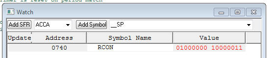
ever was before. I'm making progress at least. 20:47 - I cannot get further. Brick wall. I add a single instruction to the code, even a Nop(), and the chip refuse to work. The T3 interrupt service routine refuse to work if there are more that 12 instructions in the disassembly listing. I cannot adjust the T3 interrupt priority because adding the instruction to do so breaks the chip. I'm stuck. I think I should abandon this project or try discreet logic instead. The one last ditch thing I can try is to add some elaborate trap handling system. 21:29 - I used the debugger to look at the RCON register when the chip crashes. MPLAB reports the RCON register as
bit 14 is set which means:
Under normal operation RCON looks like this:
bit 14 is not set
22:06 - It works!
IOPUWR bit set issue is resolved by setting C30 optimization to 2. Who knew...
30 March 2012
The SAA7030 digital filter is working with dummy data. The next
tasks are to enable the Data Converter Interface on the dsPIC, convert the
samples from the DIR9001 to binary offset format, read them into a buffer and
send them out on the two (L/R) SPI interfaces to the SAA7030. The SAA7030 will
then produce samples at 14bit/176.4kHz.
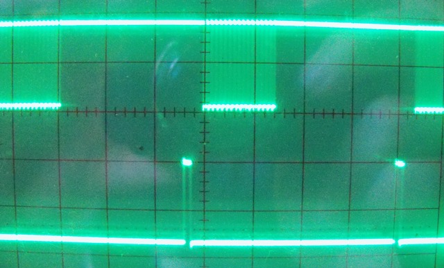
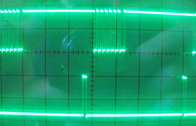
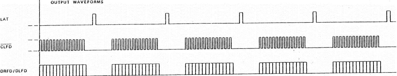
LAT and CLFD output from the SAA7030 (above) and from
datasheet (below)
STR1output from dsPIC (top) and LAT output from SAA7030
(bottom) showing how for each sample that goes in, four come out
2 April 2012
I tried getting the DCI interface to work using known good code
from my PCM-X2 as an example, but to no
avail. Will try again tomorrow. Reconfigured the DIR9001 to output data in I2S
format. I hope it's not just the compiler messing with me again.
3 April 2012
I've hit a brick wall again with the DCI. Code that is supposed
to work, don't. Code that's not supposed to work, does! I follow datasheets and
application notes to the letter. I don't get it...I research, I read, I
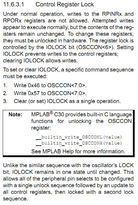
try...and still nothing. <sigh>. When I configure the RPINRx and RPORx
registers using the "right" way using the unlock sequence the chip is dead upon
reset. When I just configure the registers without the unlock sequence it works
perfectly, yet the debugger reports that the registers didn't change. BUT THE
CHIP WORKS. Huh?! This unlock sequence and its correct use appears to be a
source of great confusion judging from Google searches.
4 April 2012
I've had it. I'm tired of the dsPIC33FJ128GP802 28-pin device and
its freakishly bizarre and illogical behaviour. I've requested samples of the
dsPIC33FJ128GP206/306 and 708 64 and 80-pin devices. Thank you to Willem and
Bernd at Tempe Technologies Pty Ltd. Here's the
code that just won't work. The chip just
traps or resets or whatever. It is my hope that having dedicated pins for things
like SPI and DCI will ease development and avoid the horrible multiplexed
peripheral pins. I'm going to make a little adapter board for the 64/80 pin
dsPICs to sit on. I might get an adapter from ebay...
I ordered some adapter boards on e-bay. $12.50 for five.
28 April 2012
I've received and installed the the new dsPICs on the adapter
boards and MPLAB reports that its got comms. So far so good. I don't have time
to do any more now. I'm using a dsPIC33FJ128GP306A. I'm going to tweak the
previous code for the new chip and see if it behaves any better. Here's
hoping....
29 April 2012
01:49 AM New chip is up and
running. I now need to wire up the SPI interfaces to the SAA7030, connect the
DCI to the DIR9001 and test the code further.
30 April 2012
08:49 PM I'm making steady
progress again thanks to the better behaved chip. The DCI interface is working,
but there is still an issue with buffer management. Audio data can be seen
coming out of the two SPI interfaces to the SAA7030. This is the furthest I've
come so far. Hooray!
I love the new chip. When I tell it to do something, it does it.
It doesn't just lockup and reset like the 28-pin device does. I would not
recommend the 28-pin dsPICs for development. They're too finicky.
11:00 PM More progress. I now
have 14bit left and right data appearing at the output of the SAA7030 that
appears to correspond to the input. Drawing a picture is often the best way to
figure things out .
Goldilocks20120430.zip
11:40 PM Added the code to
convert the 2s complement format samples from the DIR9001 to the offset binary
expected by the SAA7030. I'm going to test the output of the SAA7030 using the
two TDA1540s (DACs) I have. Once I'm sure the data is leaving the DIR9001,dsPIC,
SAA7030 chain correctly I can add the chips for serial to parallel conversion.
Then finally I can add the Burr Brown DACs.
5 May 2012
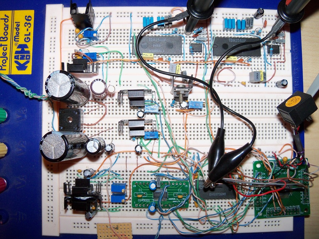
I spent some time digging through my components and junk drawer
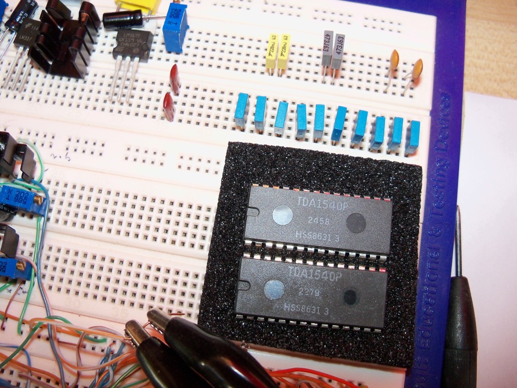
to find all the capacitors I'll need for the TDA1540 DACs. I'm using the
TDA1540s for testing as they can interface directly to the SAA7030. I still need
to buy some other odd-ball values I don't have.
7 May 2012
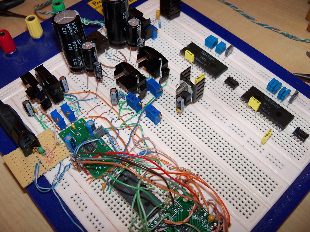
I did some more building on the DAC. The board is ending up being
more power supply than DAC as some of these old chips need some bizarre voltages
like -17V and -2.5V. For now I'll be using NE5534s for IV conversion of the
TDA1540s. That's what is used in the application circuit in the datasheet.
Output filtering will be simple RC. I just need to see if the system works, then
I can start tweaking and installing fancy filters. I still need to buy more
polyester caps for the TDA1540s.
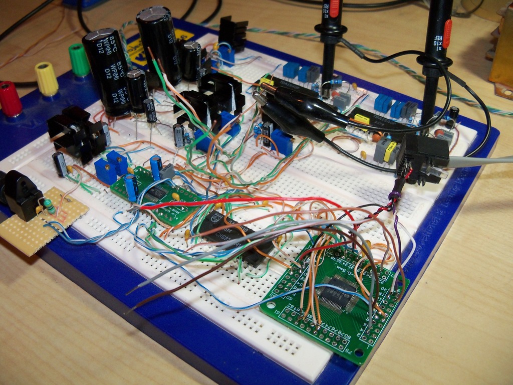
12 May 2012
01:05 AM I completed the -5
and -17V supplies for the TDA1540s. I still need to do the +5V supply. I added
more capacitors to the TDA1540s as well as the resistors.
11:50
PM I did some more building. It's a complex circuit. With my real job
getting in the way I get very little time to work on Goldie.
13 May 2012
10:00
PM Finished building. Ready to test. dsPIC dead as a Dodo. Tried
everything, checked everything. Nothing. I tested comms with a 28pin device. It
works. Have to make up another dsPIC board now.
14 May 2012
I have a fully functional dsPIC again. Now I need to reconnect
the data bus cables and hold thumbs...
16 May 2012
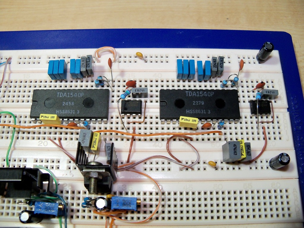
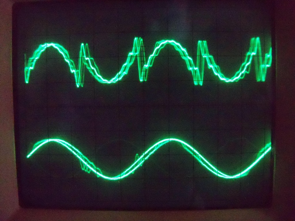
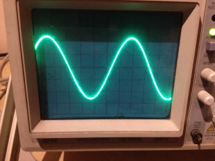
Success! Well some at least. The TDA1540s are producing something
that looks a helluva lot like the 700Hz tone I'm playing back. The scope can't
seem to sync perfectly though, so I need to tweak and test and see if it's the
scope or the data that isn't right somehow. At least I know the hardware works
so I must just check and recheck the software. I think I'll record the output
into Audacity while playing two different tones on the L and R channels. Then I
can analyze the waveform properly.
17 May 2012
A lot better. There is still some issue with the portion of code
for one channel, that perform 2's complement to offset binary conversion, not
being triggered. 1kHz tone at 0dB...
18 May 2012
I spent about 2 hours checking and tracing. No improvement. I
have some suspicions I'm going to follow up later. I think clock skew may play a
roll with the MSB of one channel being read in wrong. I
find it frustrating to work with the PIC sometimes because I need to see what is
going on INSIDE. Yes, I can use the debugger, but sometimes you'd like to just
trace and scope what is happening with the peripherals inside. Working with an
analog scope is also tricky. It would be nice to freeze a view sometimes. It's
beginning to look more and more like data isn't being clocked into the SAA7030
correctly. Keep digging...
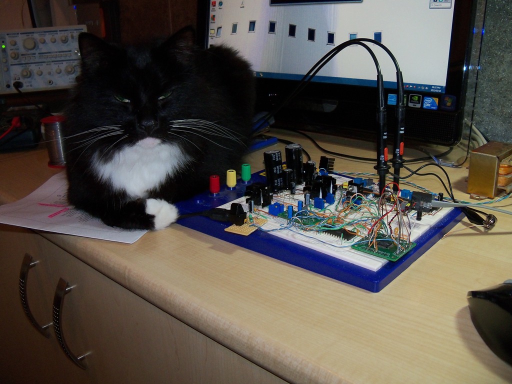
Bear approves
19 May 2012 (my birthday! )
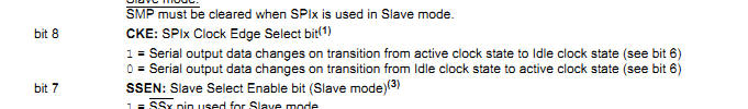
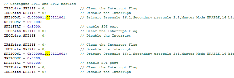
01:20 AM My suspicions
regarding the clocking of the data over SPI from the dsPIC to the SAA7030 was
correct. I changed the CKE, bit 8 of both SPI1 and 2 from 1 to 0. It improved
the situation in that both channels now have the proper waveform. There are
still occasional glitches to track down. A Left/Right/Left/Right test from the
BINK Test CD, shows that there is no crosstalk between L and R, however the R
channel exhibit glitches when idle. Perhaps a proper
3.3V to 5V translation of clock and data pulses from the dsPIC to the SAA7030
might help...Also I'll check clock/vs data alignment.
Goldilocks_20120519.zip
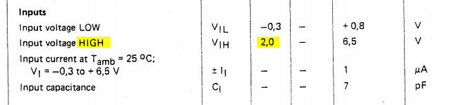
02:28 PM I don't
need to do 3.3 to 5V level translation between the dsPIC and the SAA7030. The
minimum HIGH voltage of the SAA7030 is 2V, the dsPIC gives out 3.3V. That's
enough.
From SAA7030 datasheet
20 May 2012
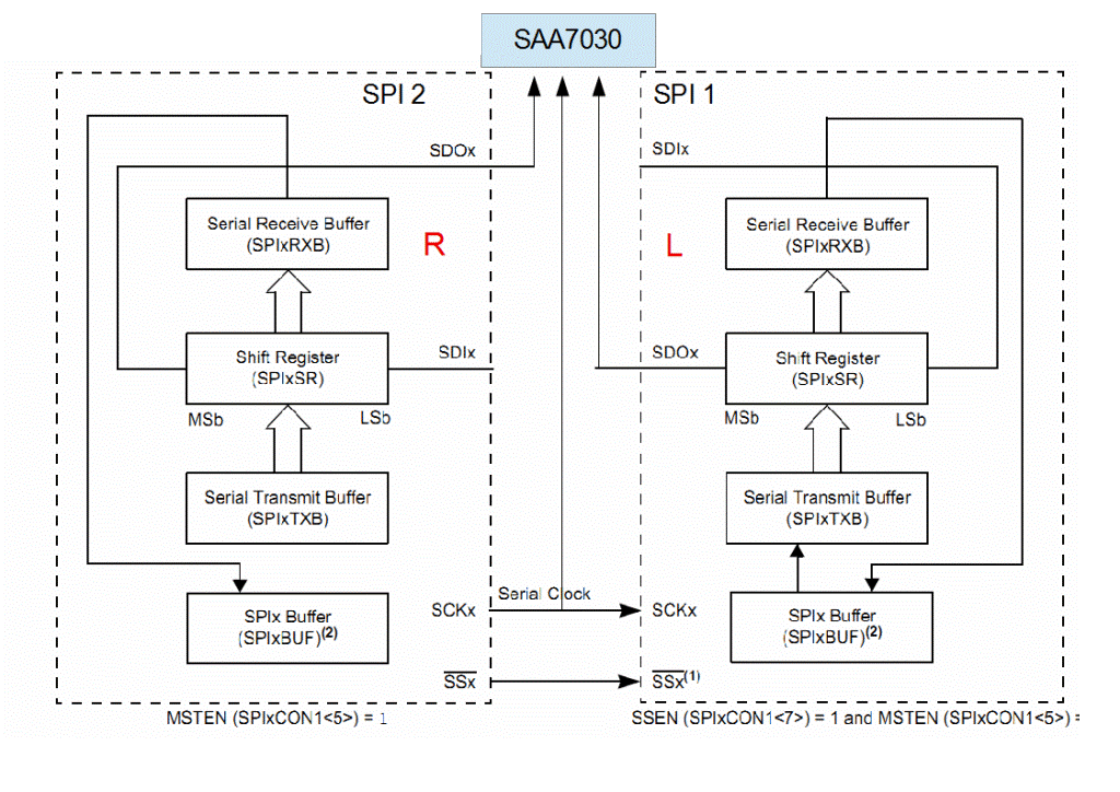
My problem till now was how to align the SPI L/R data
transmissions to the SAA7030 in time. Then it occurred to me to run the one SPI
bus in slave mode and the other in master mode. You then have the one, clock out
both sets of data. See diagram below.
In the following code snippet, SPI1BUF is loaded with a LEFT
sample. SPI1 is configured as a slave so it needs the clock from SPI2 to shift
its data out. When the write to SPI2BUF is complete, SPI2 starts transmitting.
SPI2s clock shifts SPI1s data out simultaneously. This seems to have worked as
the glitches are gone. There does still seem to be an annoying phase noise I
need to track down.
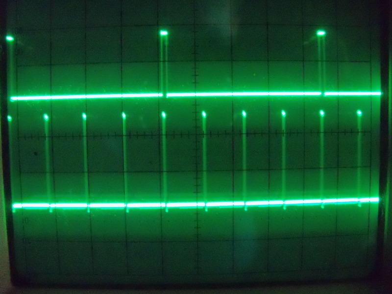
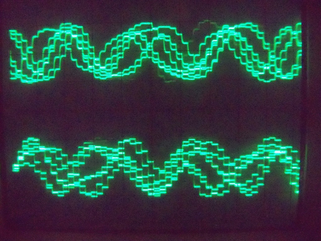
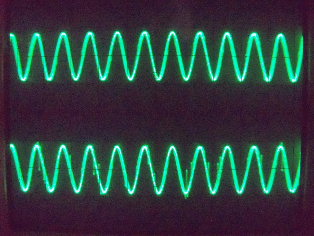
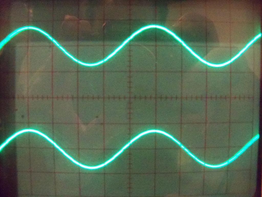
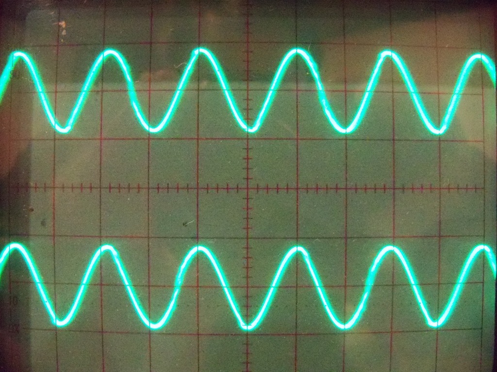
100Hz on the left, no phase noise, rock solid 1kHz on the right, some sort of "wiggle"
Goldilocks20120520.zip
21 May 2012
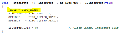
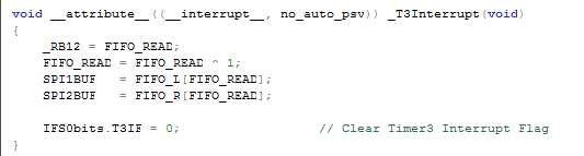
In the code below I'm using a flag on RB12 to monitor when T3
triggers. T3 controls when samples are written out. There are no timing
variations in the triggering of T3.
I had a major sniff around the circuit, but haven't been able to
find any jittery signals going to, or coming from, the SAA7030. The shape of the
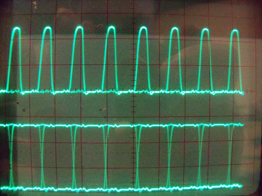
clock signal coming from the SAA7030 to the DACs is a bit rounded though. See
below (top trace is clock from SAA7030, bottom trace is data for one channel). A
74HCT04 placed between the SAA7030 and DACs can clean that up. I'm not convinced
that this can cause jittery output. I would like to try running the DACs output
just through a resistor for IV conversion to rule out any instability in the
op-amps.
23 May 2012
Using a digital scope with hold function, I've been able to
confirm that there is indeed a random and inexplicable phase shift (jump) that
happens on the output. It could be a buffer timing issue. I'll have to make some
sort of timing chart and have a look. Analyzing the timing error further I
realised that it lasts for ~50us. This is significant because 1/Fs = 22.67us
which is about half of 50us. This could indicate, perhaps, an interrupt being
delayed. It is also interesting that I'm using a 2-position buffer capable of
holding 2 samples/channel or 45.35us of sound.
50us/div
Notice how the discontinuity last for ~50us
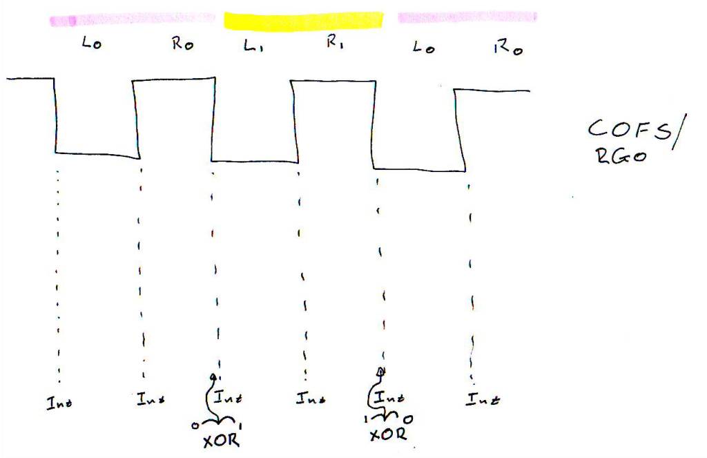
Timing of DCI module reading data in from the DIR9001
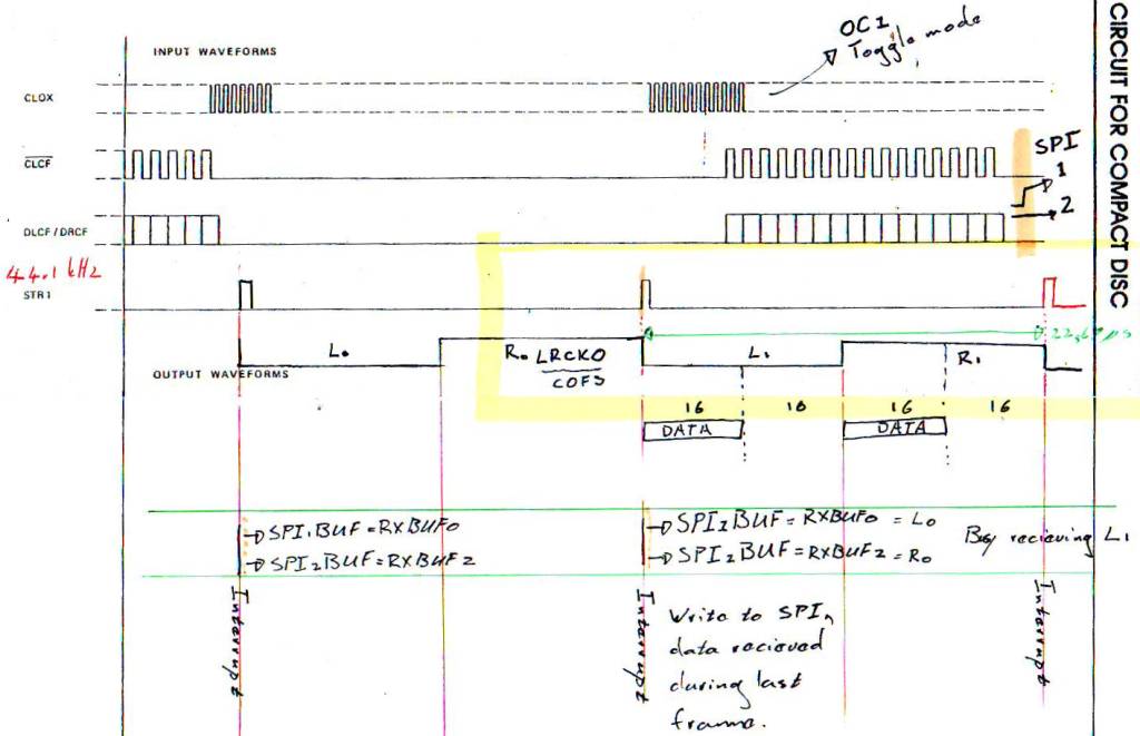
I worked out a completely new data transfer scheme between the
DCI and SPI modules that doesn't involve the use of an extra buffer. A left and
right sample is buffered by the DCI module during one frame in RXBUF0 and RXBUF2
respectively. When the DCI interrupt triggers, these samples are written to SPI
1 and 2, while a new value for RXBUF0 is being received. STR1 is COFS applied to
the DCI module except it'll be inverted by a 74HCT04. I
still have to test this.
Timing Diagram for DCI and SPI
This code falls away. There is no more buffer and
read/write pointers
No need for this code either, no more STR1 being
produced. LRCKO from DIR9001 used instead (inverted)
26 May 2012
I've been trying different things, but I've only had limited
success. Now it would seem like the dsPIC wont run, at all. It talks to MPLAB,
but even old known good code wont run. I checked the configuration settings. The
buffer is definitely not needed. As the diagram below shows, samples are read
straight from the DCI buffers into SPI every time T3 interrupt occurs.
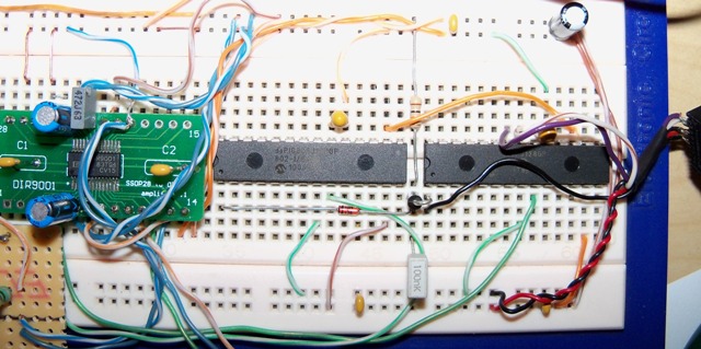
I've put the circuit aside for now. I'm a bit sick of it. I actually might just do the interface and conversion using discrete logic instead. I just want something that works. Using surface mount one can make the glue logic very compact. Once one has the logic circuit, it can be transferred to FPGA/CPLD. See the diagram below.
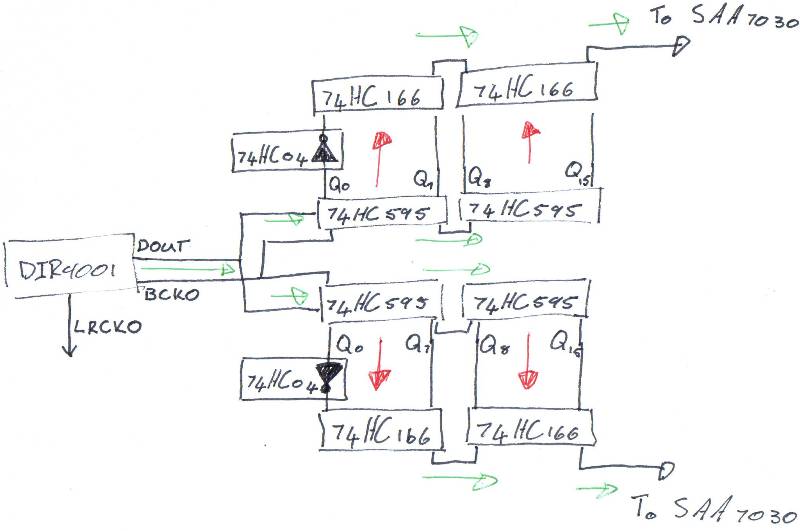
L and R samples are clocked out of the DIR9001
serially and alternately into to serial to parallel shift registers (74HC595).
This will produce two stored samples aligned in time. These samples are fed into
a parallel to serial converter (74HC166), but with the MSB inverted using a
74HC04.
Data is then clocked out in sample pairs to the SAA7030 digital filter.
I see someone in China (or eastern anyway) has developed a CPLD
based converter to sit between an SPDIF receiver and a SAA7030. It's all in
Chinese and I have no idea what's going on. I did manage to get an e-mail
address and did get a response. The thing is that I don't actually care too much
about the glue logic. I'm interested in the digital filter, DAC and output
filter part. That's interesting.
30 May 2012
I've made contact with the guy in China who sells the chip above.
$51 for two with shipping. No thanks! I'm not paying that money for something I
can do myself. Besides I won't learn anything new if I just buy it. I'm looking
to get a
CPLD
on a dip adapter along with a JTAG programmer. I'm currently downloading the
Xilinx ISE WebPACK Design Software. I'm looking at a
programmer and
board. There's also a vast selection of boards on ebay along with
programmers. I just need to learn
VHDL, which can only be a good
thing. Also, people seem to be doing
weird things to their Xbox consoles with these things.
I also want to make the design more permanent. To that end I'm
also planning on ordering some Roth
Elektronik prototyping cards. They're neat and have mounting holes. I can
mount these boards in a chassis with a power supply.
I love it when a plan comes together
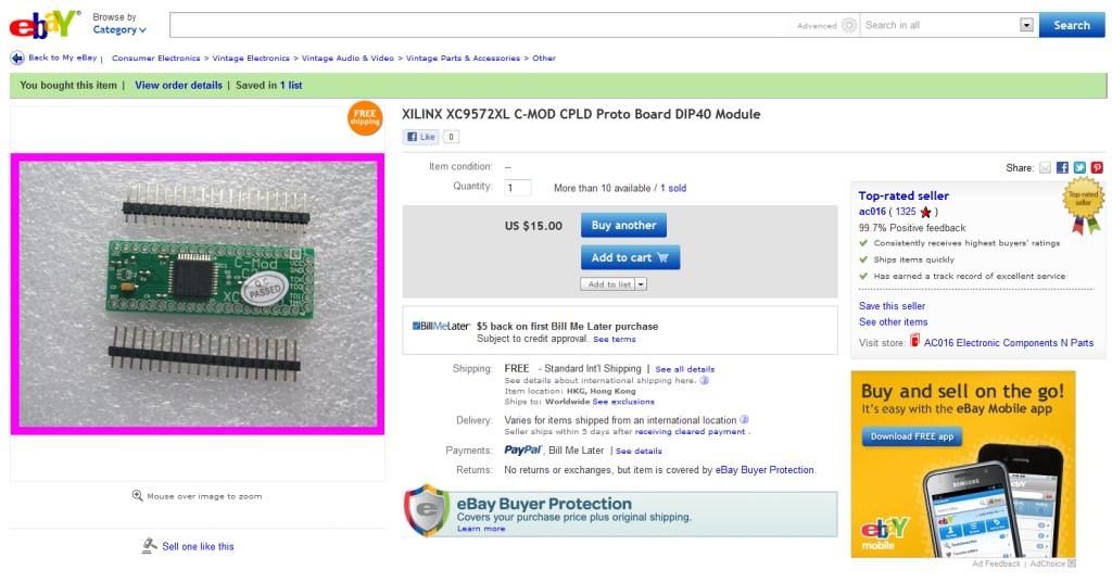
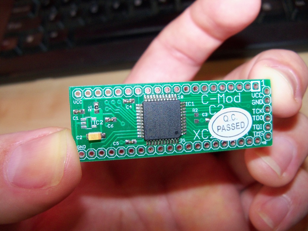
08:57pm I bought a
Xilinx XC9572XL board on ebay.
15 June 2012
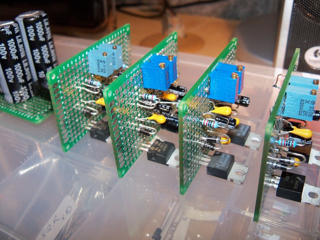
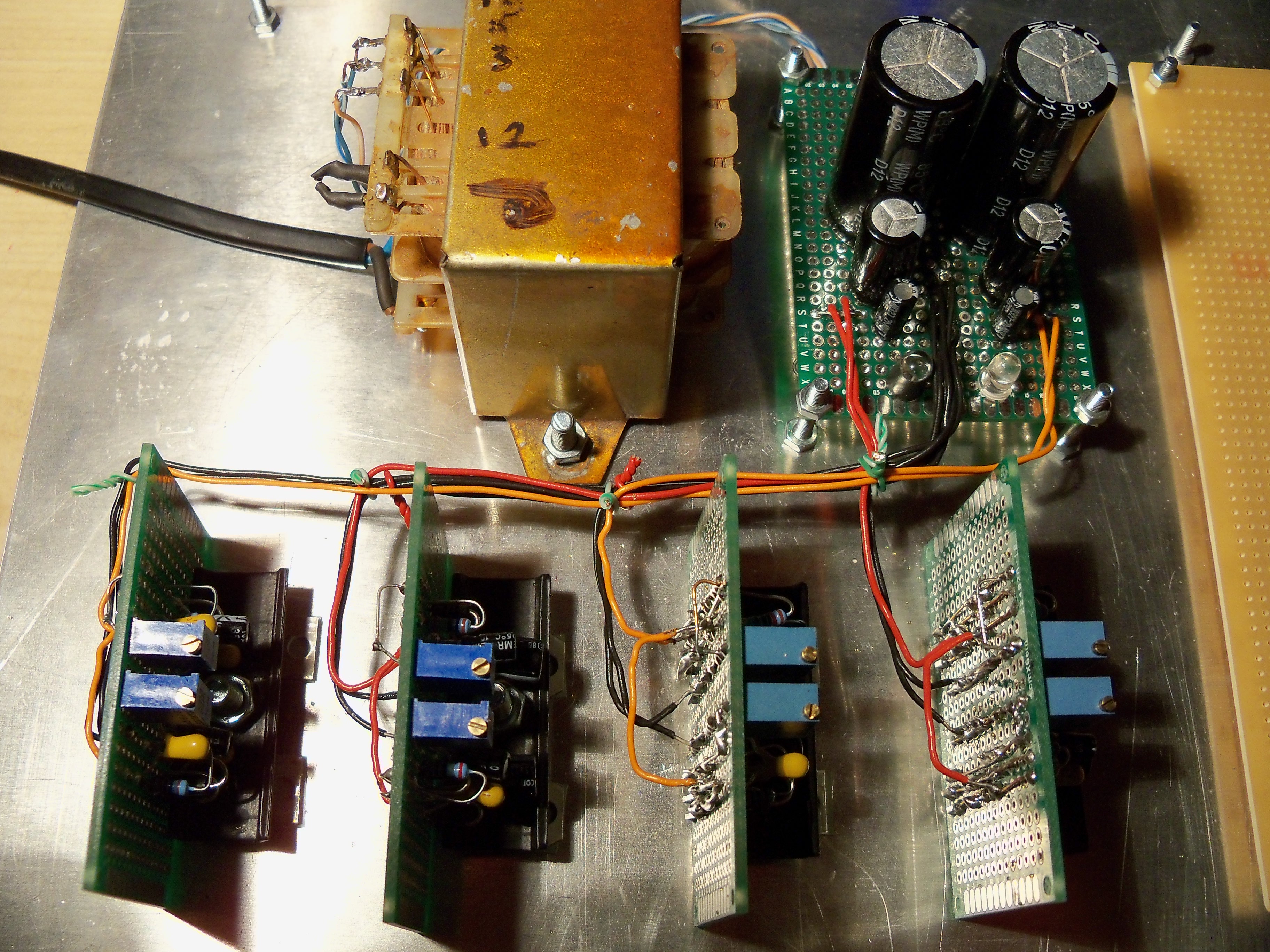
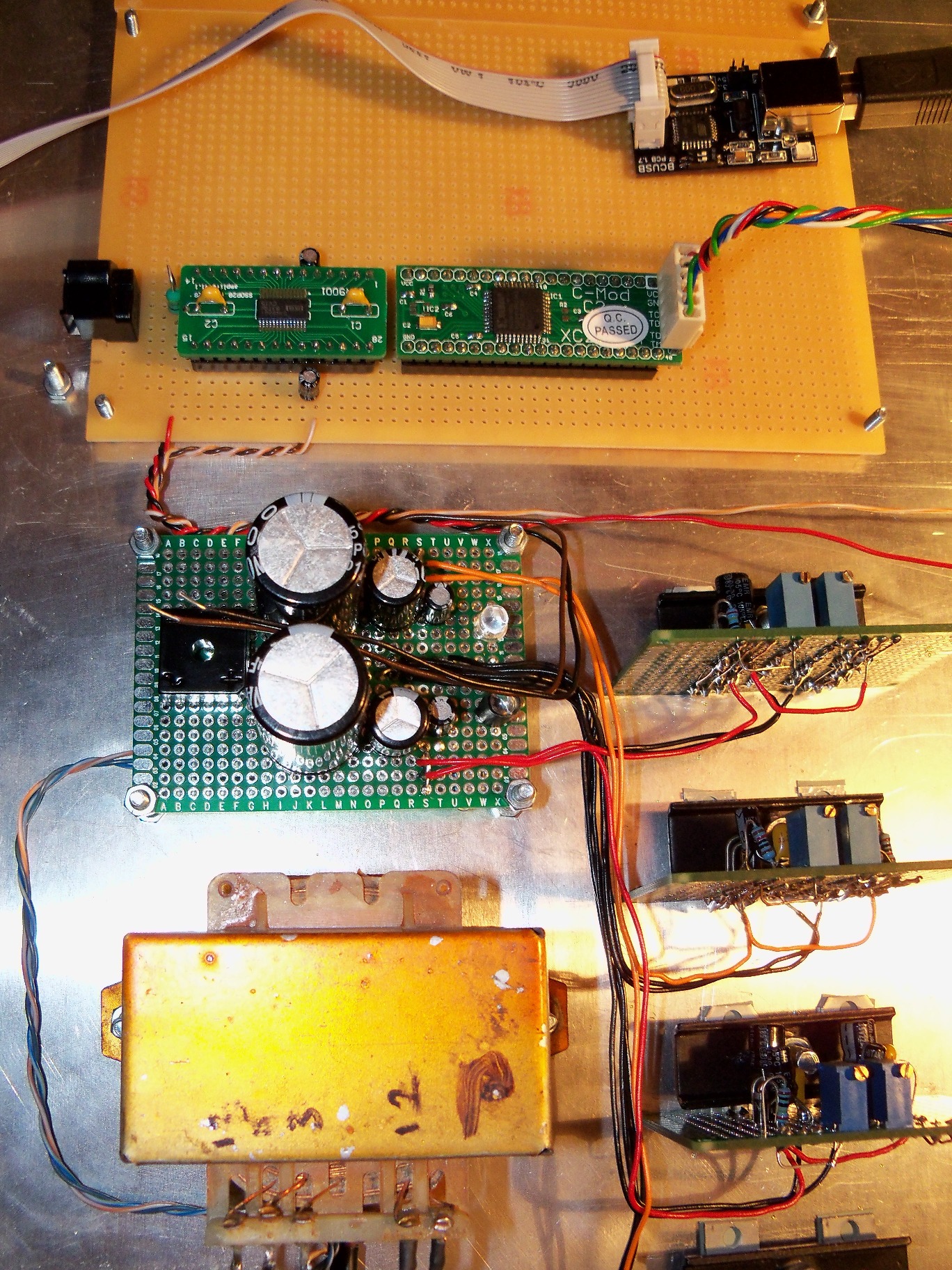
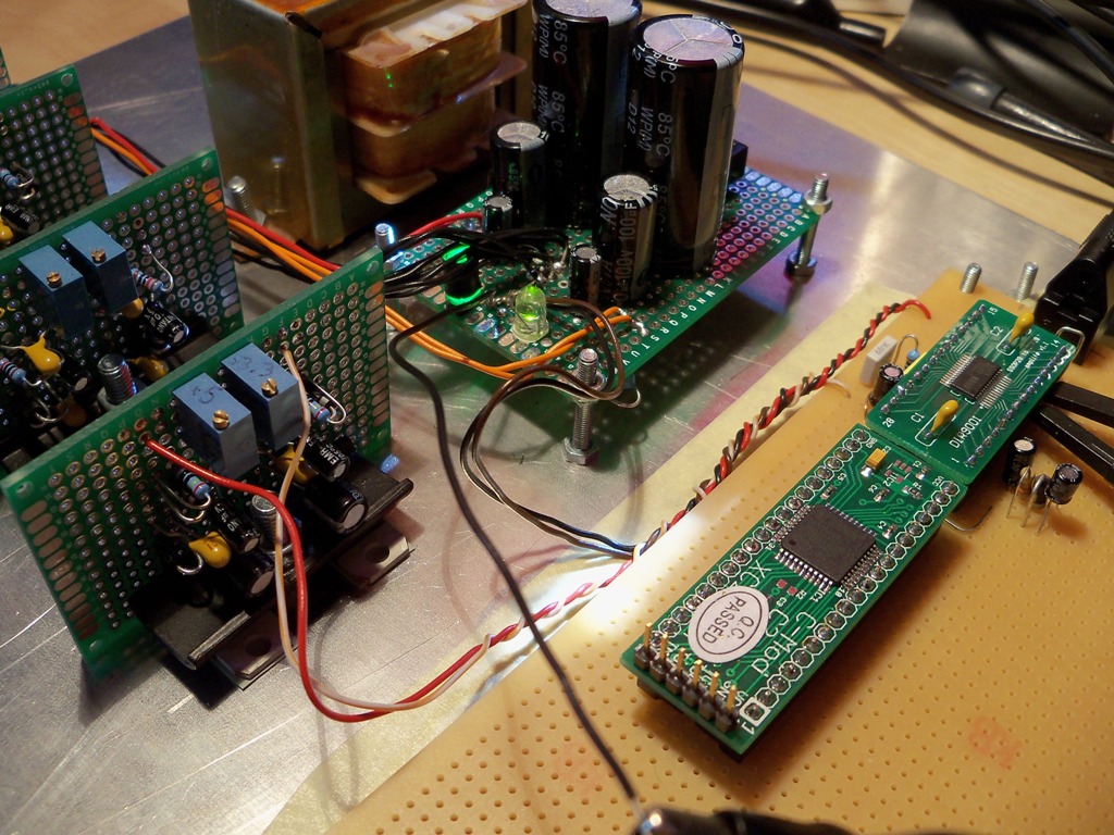
I'm getting ready to construct the chassis for the DAC. To that
end I have planned the layout. The little upright boards in the picture below
are the power supply regulators. They will be mounted as you see them with the
regulators using the 3mm aluminium base sheet as a heatsink. 4 LM317s and 4
LM337s are used to provide the variety of voltages the unit will need.
21 June 2012
My Xilinx XC9572 board and
BlackCat USB
programmer arrived. I managed to get hold of the service manual for the Philips
CD100. It contains a circuit diagram of the CD100s analog output stage. This
would allow me to duplicate the digital filter, DAC and analog output stage of
the CD100 on this project if I wanted to. The DIR9001 decodes the de-emphasis
indication bit, so I can implement de-emphasis.
Xilinx board left, and programmer right
CD100 playing ABBA The Visitors. I also have an
original copy of this disc from 1982
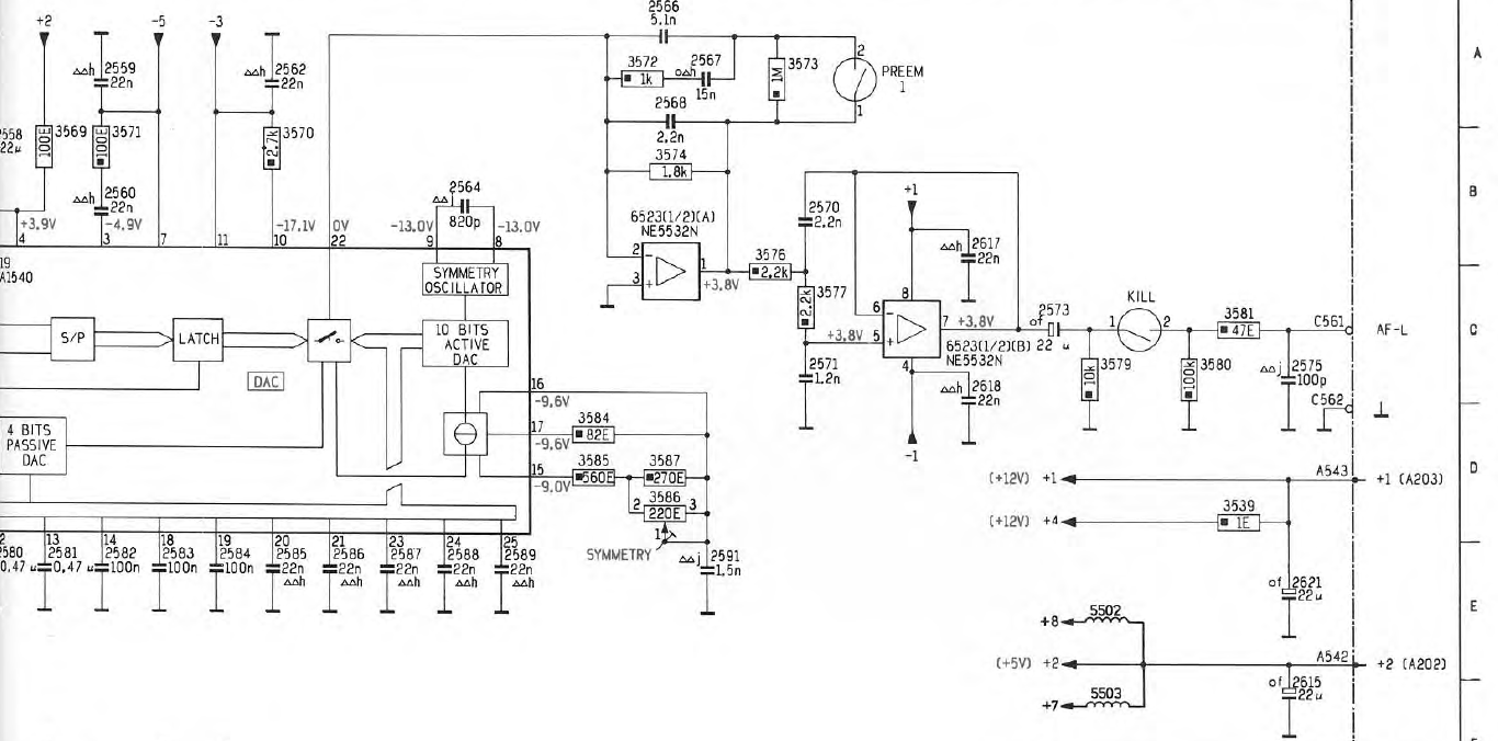
Output stage of CD100 with TDA1540 on the left. On the
right is the IV converter with a selectable de-emphasis response. Following this
is a further low pass filter stage. The symmetry adjustment at the DAC is to
ensure that both the left and right channels are the same amplitude.
29 June 2012
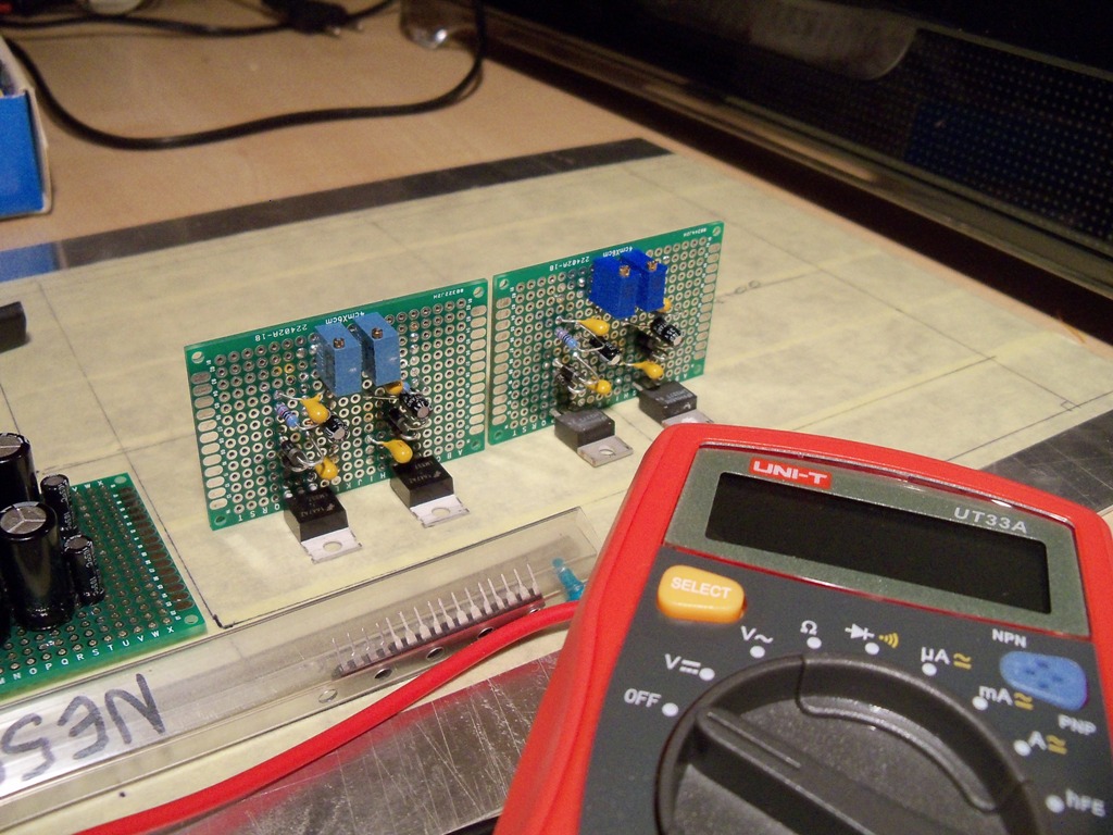
I finished two Negative Regulator modules. I also bought a new
UNI-T multimeter.
2 July 2012
Regulator boards finished and tested.
4 July 2012
Made great progress with the chassis. Regulator boards mounted. I
can do some wiring tonight.
10 July 2012 Finished construction and testing of the
power supply. I'd like to get the optical interface, digital receiver and CPLD
chip working by the 16th.
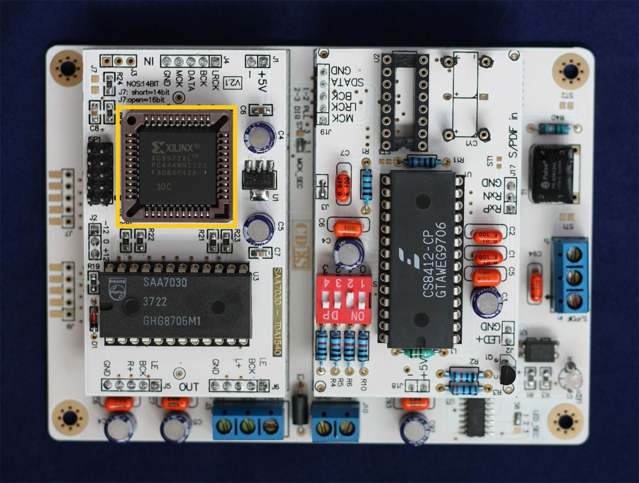
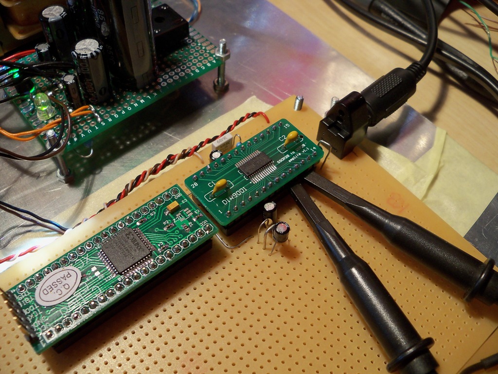
15 July 2012 Steady progress. Optical receiver, DIR9001
and Xilinx CPLD installed.
17 July 2012 The DIR9001 and optical receiver is
working. I also added a power-on-reset circuit to the DIR9001. Next I need to
see about getting the CPLD
running and writing the VHDL
code.
18 July 2012 I'm busy trying to get to grips with Xilinx
ISE Design Suite Schematic editor. I'll be entering the design using the
schematic design feature. The learning curve is quite steep, but I'm making
progress. Fortunately there are plenty of examples and tutorials. Work on this
will have to stop for a while as my "real" job starts again next week.
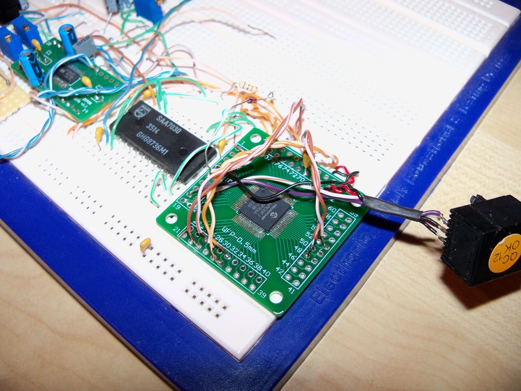
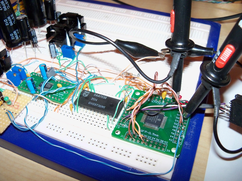
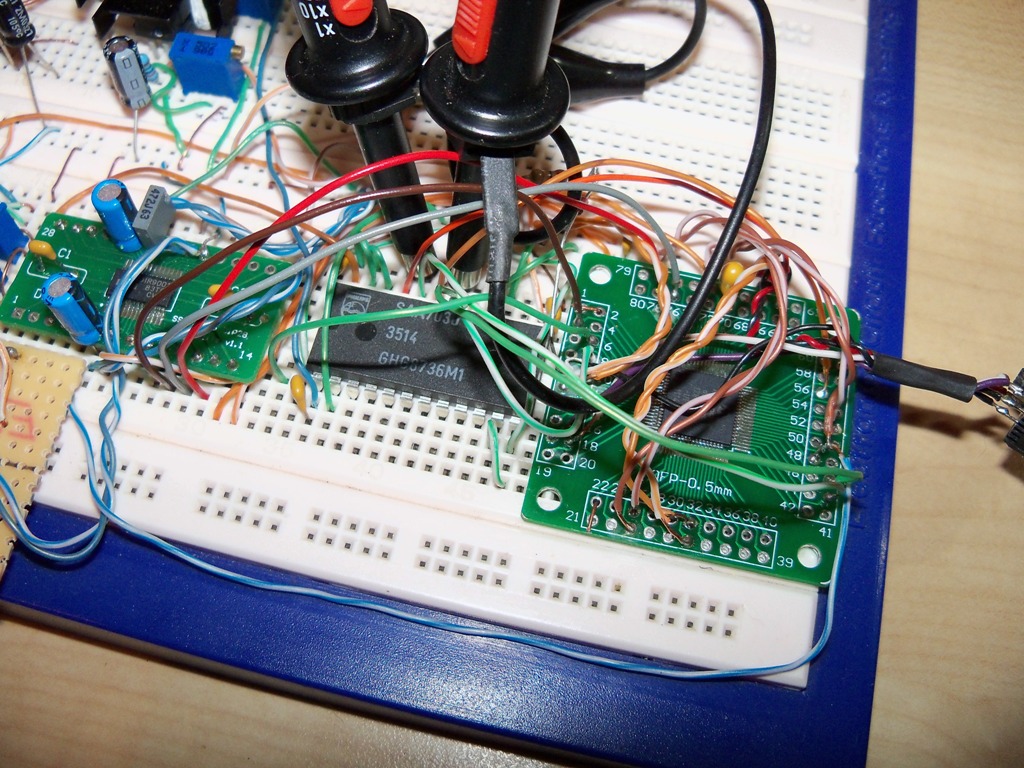
18 September 2014 I want to return to this project. I've ordered a
sample conversion
module from china. Cost is $25. I can do my own discrete conversion, but I
don't have the time or the energy. I'm more interested in the DAC and output
stages anyway.
30 April 2020 While working on my PCM-3
processor I made a little departure and used one of the BURR-BROWN "Gold"
DACS to build a function generator driven by a dsPIC33.
Waveforms read from dsPIC33 RAM
|