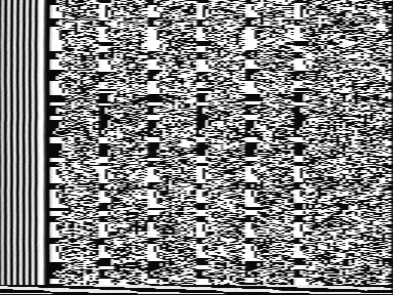
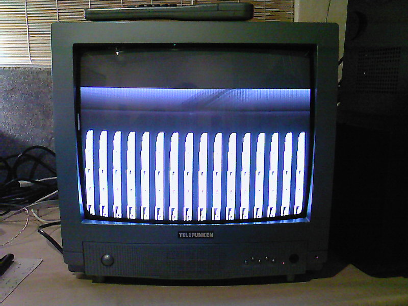
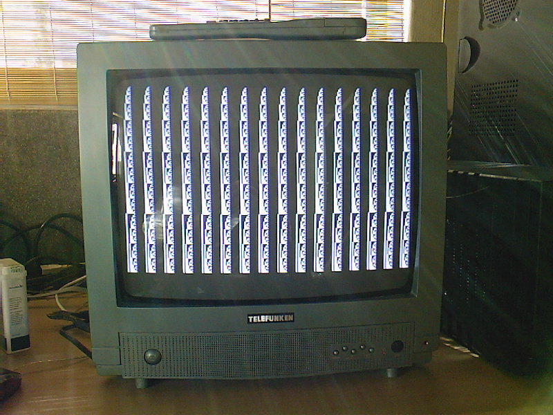
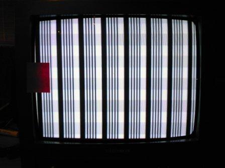
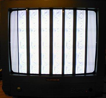
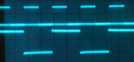
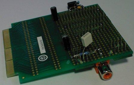
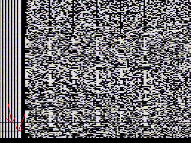
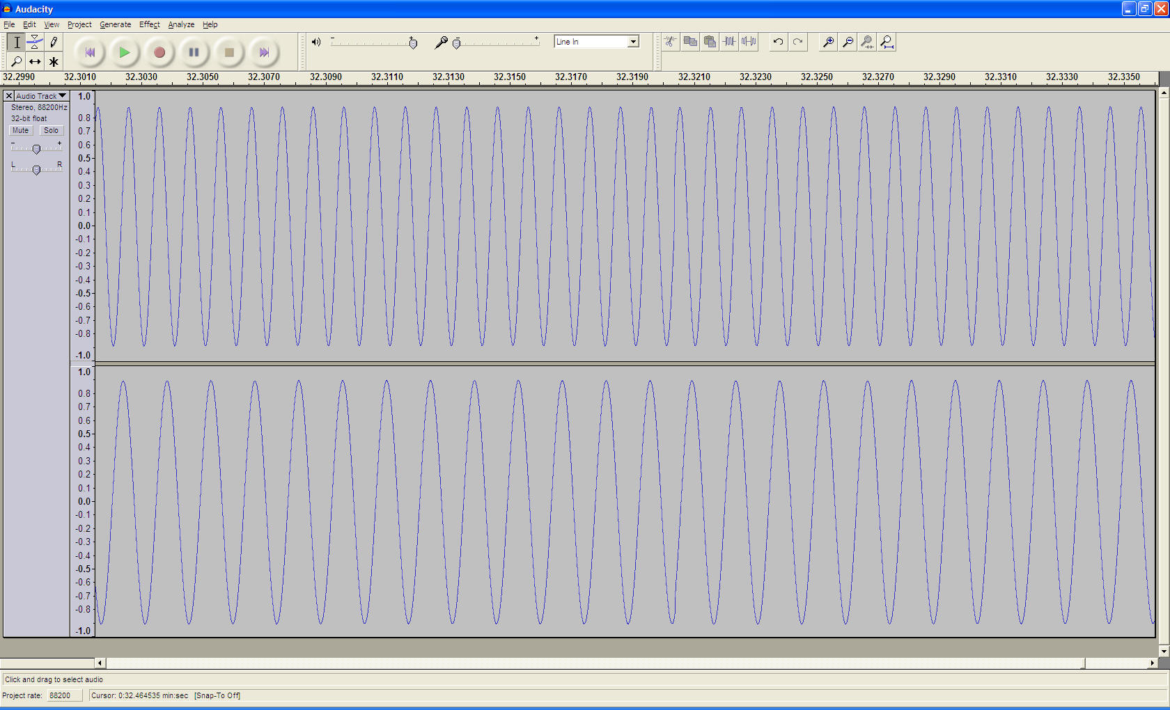
| PCM-X2 Processor updated: 2022/12/03 09:22:13 am GMT+2 The PCM-X2 is an experimental device I developed to record uncompressed 16 bit PCM stereo audio, sampled at 44.1kHz, to the helical video tracks of ordinary VHS video tape. This device can essentially turn any video tape recorder into a Digital Audio Tape recorder. The output of the PCM-X2 is similar to the output of the Sony PCM-1630. The PCM-X2 produces a video signal with audio data embedded onto it. This video signal is treated just like any normal video signal by a VCR. Below is a sample of one video field (20ms) containing 28224 bits of audio data, 294 lines x 6 samples x 16bits/sample
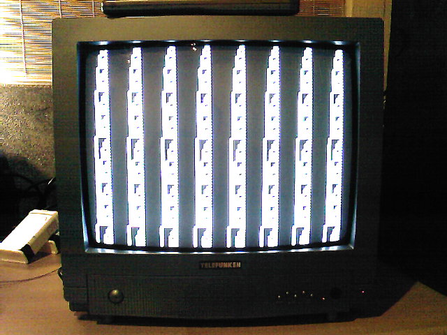
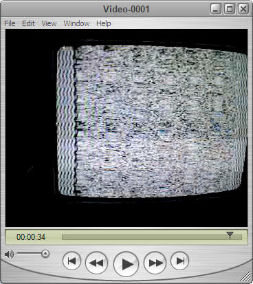
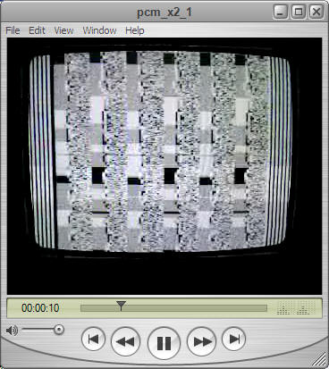
PCM audio data as recorded on VHS video tape. From left to right the columns are, clock sync word, 6 samples LRLR etc, checksum PCM-X2 playback test_10012009a_3.mp3 *music tracks used for demonstration/educational purposes only under fair use policy. 18/05/2010, Digital Audio Playback test from VHS tape
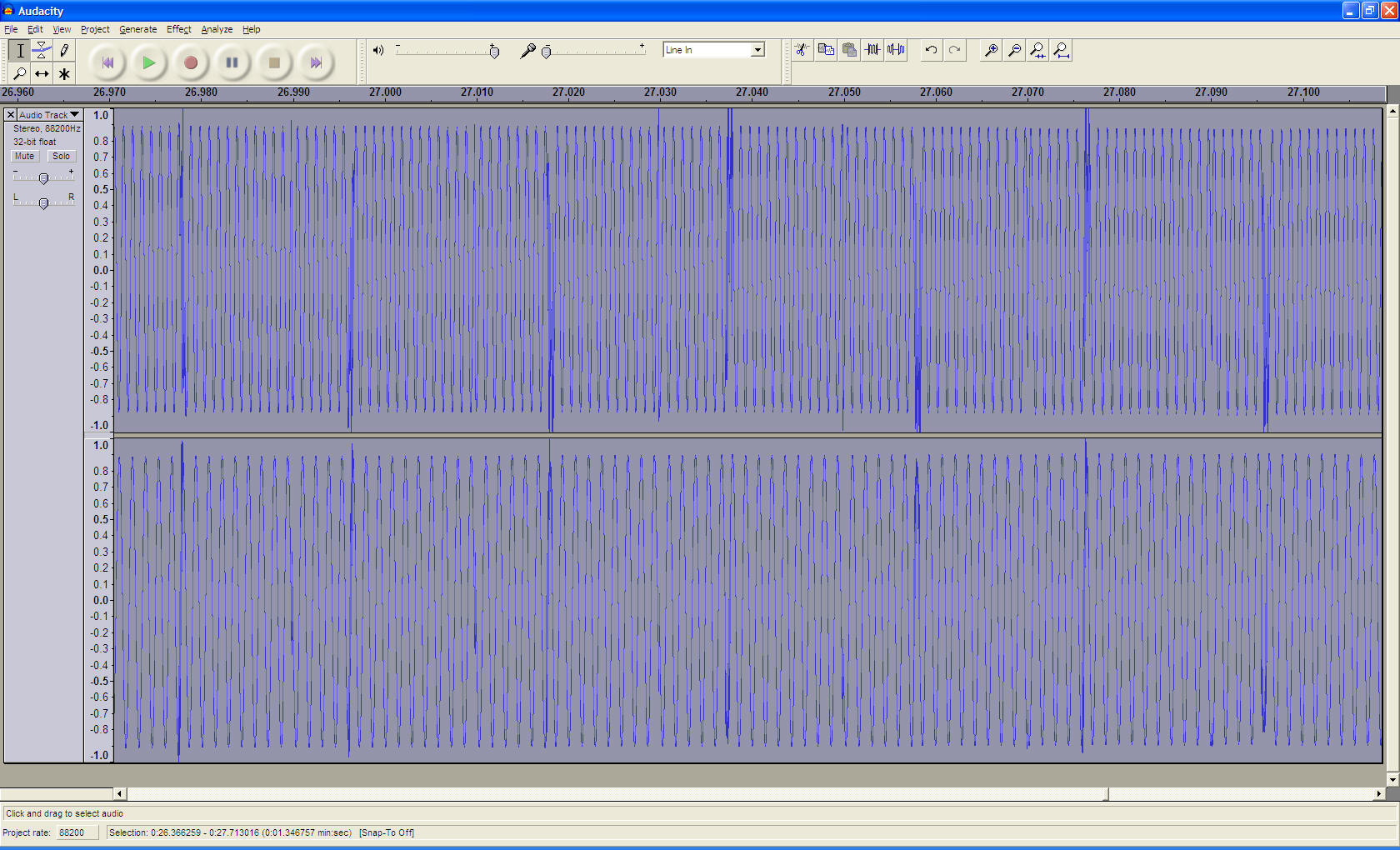
09/05/2010, Latest test with improved code. Still occasional glitches.
Early test, 14/01/2009. The buzzing during "STOP" is due to the FIFO buffer contents being read out over and over again. It is not present during normal playback. *music tracks used for demonstration/educational purposes only under fair use policy.
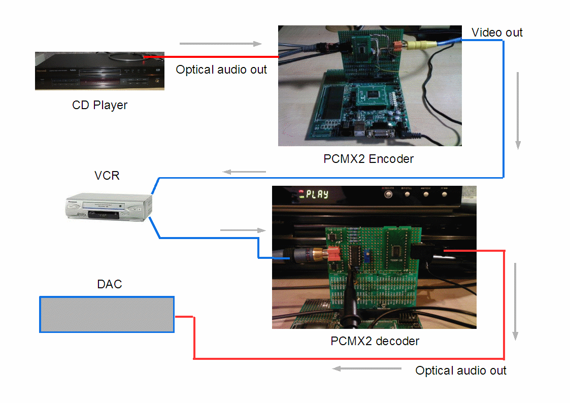
The purpose of the PCM-X2 is to develop a device to convert PCM audio into a pseudo video signal suitable for recording onto video tape. This will allow any analog VCR to act as a DAT recorder. My goal is to build a PCM processor that can connect to any PAL video recorder with at least 240 lines of horizontal resolution. The PCM-X2 builds on the knowledge gained from development of the PCM-X1. The PCM-X1 used a mixture of two microcontrollers and discrete logic. The PCM-X2 uses a single dsPIC33 along with some ancillary interfacing circuits. Specifications (encoder) Specifications (decoder)
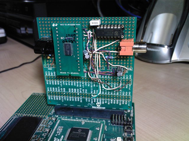
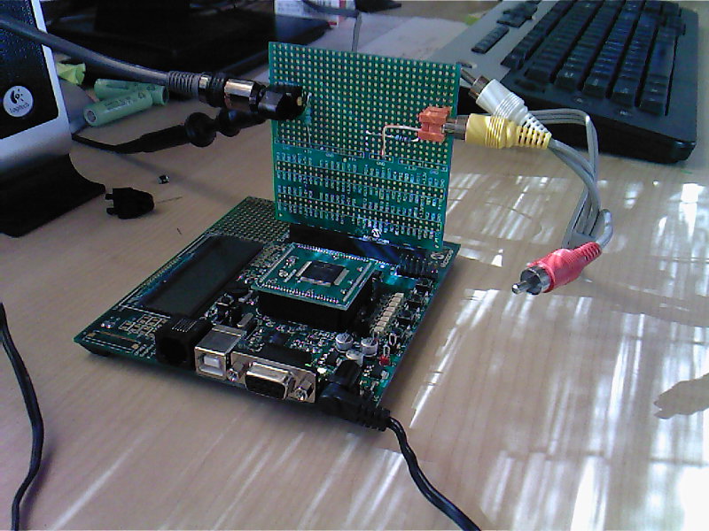
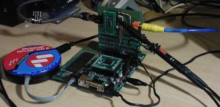
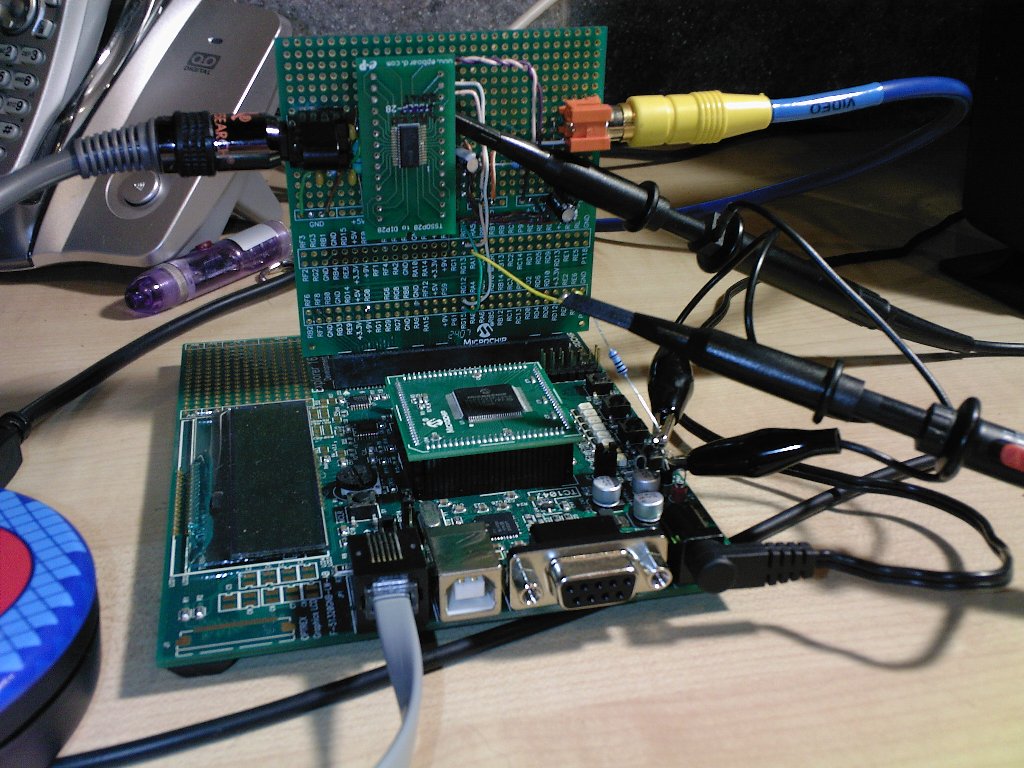
Development Blog 12 January 2008 I nearly have all the pieces I need to start development of the PCM-X2 encoder. I have the PIC16 Development board with PIC24 and dsPIC33 processors. I also have the In-Circuit Debugger. I'm just awaiting a new PICkit2 programmer. My last one was stolen. Some burglar thought it was a flash drive or something... The Explorer 16 development board I'm using has a handy expansion slot for which I want to make a card with S/PDIF reciever/transmitter to feed samples to and from the dsPIC33 as well as video in/out. The idea is to do all the processing I did in hardware with the PCM-X1 in software for the PCM-X2 encoder. The dsPIC33 has many handy hardware features that make working with PCM samples a lot easier. If you're looking for a great how-to book on coding the PIC24 in C, then try "Programming 16-bit Microcontrollers in C". The author, Lucio Di Jasio, provide many useful support and development tools on his companion website. One of these are PAL and NTSC video libraries that'll generate the timing signals for you. I'll have to tweak these though as they are designed for displaying computer graphics on a TV. This means that the composite sync is generated in such a way that the displayed image is not interlaced. This is done in to reduce flicker. To properly record the pseudo video signal with the PCM samples in it I want it to conform to the CCIR 625 line standard. 26 January 2008 I received my replacement PICkit 2 programmer and also some Prototype PICtail Plus Daughter Boards. I'm planning to construct the interface circuits on one of these boards containing:
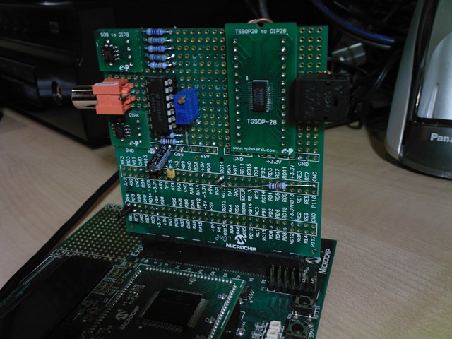
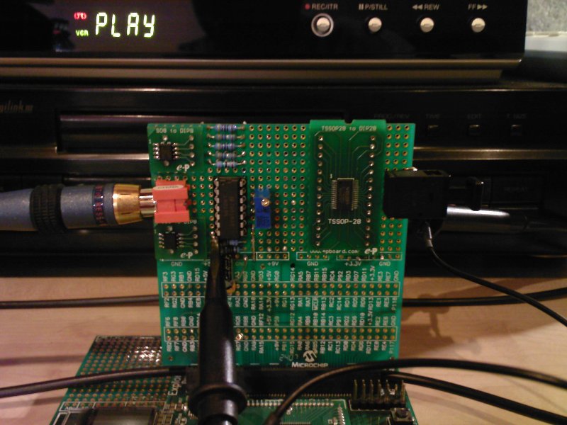
20 February 2008 RAM requirements for the dsPIC33: From the calculations for my PCM-X1 I know that one video field stores 28224 bits. The PIC will store a video bitmap of the PCM audio in RAM which will be read out sequentially. This means that the PIC needs 1764 bytes or 1.8 Kbytes of RAM for a single field video bitmap. Considering the dsPIC33FJ256GP710 (the chip in my kit) has 30 Kbytes of RAM this should be OK. 26 April 2008 I've started construction of an optical SPDIF interface for my PIC development board. I'm using a TORX177 Toslink module along with a Burr Brown DIR9001 SPDIF decoder chip. The DIR9001 is in a TSSOP-28 package so I had to order a TSSOP to DIP converter from epboard.com
I'll install the DIR9001 once the TSSOP-DIP adapter arrives. I've discovered that the dsPIC33 has a very handy Data Converter 29 April 2008 Added the components around the TORX177 Toslink interface, capacitor and inductor. Also connected the TORX177 to +5V. Connected the composite video output as well. Still have to install the DIR9001. The hardware this time round is much simpler as all of the processing will be done in software. I don't have to develop any new code to generate the video output either. The book I'm using, Programming 16-bit Microcontrollers in C, contains complete NTSC and PAL video sync generator C code as well as code to display a bitmap stored in RAM on a video screen. The only new code then would be the code to read in PCM samples and store them in the video bitmap in RAM. At this point I would also like to add interleaving as well as error correction coding.
1 May 2008 I connected up everything and loaded some video test patterns for the PIC24 to display but to my dismay:
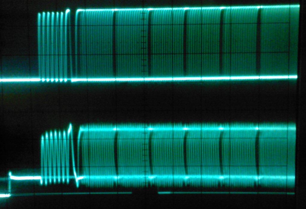
The TV would not sync properly. The video routine I'm using comes from the book "Programming 16-bit Microcontrollers in C". The author simplified the routines for generating the vertical sync pulses. So they're not standard. I figured the TVs' vertical retrace wasn't being triggered properly so I altered the code to generate standard vertical sync pulses. This was quite an involved process which involved changing state machines and adding Output Compare interrupts. It made no difference. Here's my version of the C code: The authors version: After much digging, desoldering and even altering of code I traced the problem to a power supply issue. I'm now using a proper bench power supply and the circuits seem to be happy.
2 May 2008 Tested the output of the authors' GraphicPAL.c module. It produces horizontal sync pulses with proper PAL video timing of 64μs per line, 312 lines per field and one field every 1/50s. The only difference is the shape of the vertical sync and pre-and post equalization pulses. It's also non-interlaced. The VCR and TV I have sync up very happily with this slightly non-standard video signal. The code is much simpler, so I'll stick to using this video module as a base to build my project on. If I find later that some VCRs won't sync properly I'll have to go to the more complex code that generates perfect CCIR-625 video timing and pulses. More complex code will need more RAM though. Here's a good coding and engineering lesson: Keep simplifying until it stops working. Then take one step back. 3 May 2008 I've completed the code to produce standard PAL 625/50 video sync pulses. By using standard video timing I'll avoid compatibility issues in the future.
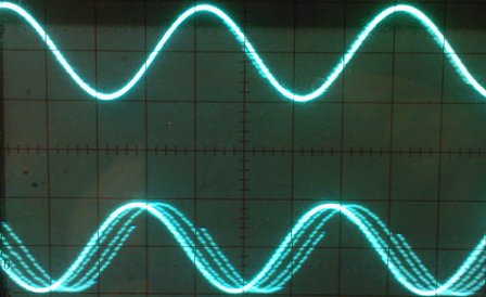
Stable interlaced PAL video
Vertical sync pulses with pre- and post equalization, field 1 and 2
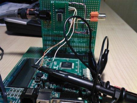
16 May 2008 I got the DIR9001 SPDIF decoder working. I can now access the PCM samples.
The way things look now. The optical input is on the left with the DIR9001 on an adapter board.
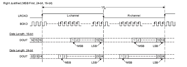
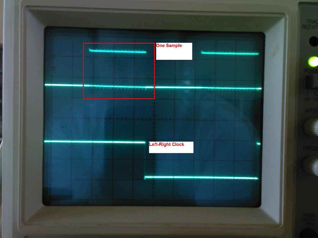
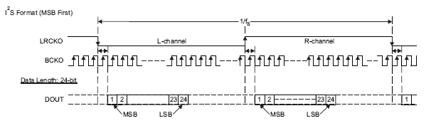
The LRCKO and DOUT output from the DIR9001. A single sample is indicated. MSB is on the left. 17 May 2008 Modified the settings of the DIR9001 to output samples according to the I2S (Inter IC Sound Protocol) protocol. This is what is expected by the DCI interface on the dsPIC33.
I2S format 28 May 2008 Ported the video code successfully to the dsPIC33FJ256GP710 and created a simple test pattern to test the SPI module. The dsPIC33 is running at 40MIPS. The previous PIC24 ran at 16MIPS. What's next? Create a FIFO buffer in RAM to read samples in from the DCI module and clock them out via the SPI module. I'm using a simpler non-interlaced video generator routine. I noticed that a video recorder locks on to the non-interlaced video signal just fine.
10 August 2008 Development of the PCM-X2 encoder has stalled somewhat due to work demands. Here is an archive of my development code so far. It includes debug information as well. I created code to test the operation of a software based FIFO buffer along with the video modules. I initially had problems with buffer underruns during my simulations. I traced the problem to the fact that the video module was generating video fields to quickly (19.968ms/field instead of 20ms), thereby causing the FIFO buffer to eventually empty out. This happens because the number of PCM samples per line is fixed. I refined my video code to generate interlaced PAL video at the exact rates of 64us per line and a field rate of 50Hz. Simulations confirm this. I now have to add FIFO buffer and I2S code to this interlaced video module. I'm going to create some test programs to get to grips with the operation of the DCI and I2S before I add it to the video modules. This'll make debugging easier. PCM-X2 encoder_development_code 24 August 2008 Did a bit more work. Mostly checking the interlaced PAL video module and cleaning up the code. Simulated the video code to check for proper video timing.
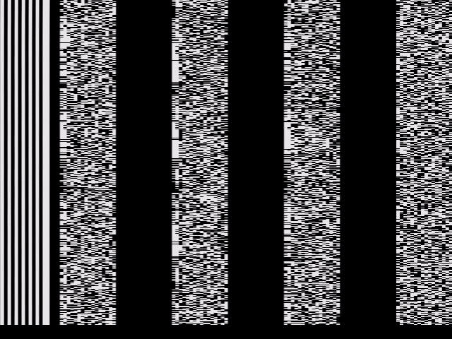
25 August 2008 Tweaked more code. I have an interlaced PAL video module running now. The code has a FIFO buffer. Right now this is filled with dummy values which is then clocked out. The picture below shows the 8 unload slots in each video line. Only slots 2-7 actually contain data. Slot 1 will contain a clock run-in. Slot 8 will be reserved for future use and can conceivably contain any auxiliary data.
Before I can go any further I have to first figure out and test the DCI module and I2S interface to the DIR9001. I have an example from Microchip that I'm gonna take a look at. 27 August 2008 I'm slowly beginning to understand I2S. It helps to decode and understand the examples from Microchip. 30 August 2008 OK. I finally figured out I2S. I took the sample code from Microchip and removed the DMA stuff, to simplify, and started tweaking. I now have a working I2S interface that reads samples in and then transmits them out. It's a simple test, but it helped me understand what's going on. Have a look at the debuginfo.txt file in the ZIP archive. Here's the code:
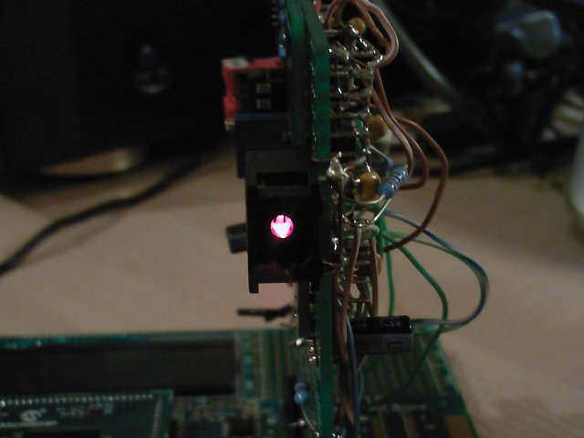
The thin yellow wire in the middle of the photo comes from CSDO/RG13. You can also see the pull-down resistor I had to ad between CSDO and ground. The DIR9001 is visible on its' adapter board with the optical input on the left and video out on the right. The laser diode in the back is a favourite toy for my cat.
The dsPIC33 I2S output. BCKO/CSDO is at the top and LRCKO/COFS at the bottom. The top waveform shimmers and changes as the sound data changes. Below is a diagram for reference purposes.
1 September 2008 I had a look at the specs of different dsPICs. I should be able to make the PCM encoder unit very small using the 28 pin dsPIC33FJ128GP802 instead of the 100 pin device I'm using now. The only other chip would be the DIR9001 and that too is a 28 pin device. The component count would actually be very low as I'm doing all the real work in software. If I space everything correctly, the PCM-to-video encoder unit could be the size of a matchbox. This is a far cry from the Sony PCM-1. To be fair though the PCM-1 had a DAC and ADC unit. My unit will require external DACs and ADCs connected via TOSLINK. 2 September 2008 I ordered some samples of dsPIC33 controllers from Microchip as well as some Digital Audio Reciever and Transmitter chips from Texas Instruments. I don't pay for chips. There are many manufacturers who are willing to give free samples of their products to hobbyists like me. This means in turn that when it comes to production I'll be more likely to be loyal to the manufacturer who allowed me to try his wares for free. I guess that's the idea. Nobody's going to try your chip to see if it suits their application if you charge them a lot of money just to play with it. It would be unethical to use samples in a production version of my PCM processor, so I'll buy the chips when that moment arrives. I ordered samples of the DIR9001 from TI.com as well as the DIT4096. I've started applying my mind to how I'll decode the video information coming from a VCR back into a digital data stream. Looking at the video waveform from my PCM-X1 after it's been recorded: One could recover the sync pulses from the video waveform and use them to trigger an interrupt on the dsPIC to extract the data. It would still be necessary to employ wave shaping to extract a clean digital signal from the waveform. I noticed that the dsPIC has comparator units which may prove useful when it comes to actually processing the analog video into a data stream. To reduce the chip count one can even do away with using the sync pulses altogether. I would prefer to actually employ synchronization and start-of-frame bits before the data, because with VCR's the sync isn't always reliable. This would have the advantage of reducing the chip count. I can the use routines similar to application note TB045 from Microchip. The dsPIC periodically samples the recovered data stream looking for edges and special bit patterns to indicate SYNC and start of frame. This would be more reliable as the system should be able to compensate for jitter in the VCR output. By using a stream of SYNC bits in a 1010101010101010 configuration at the beginning of each line, the system will resync its' clock every 64us. This can be followed by a start of frame delimiter of say 0000000010101011. The dsPIC can then count 6 samples after the frame delimiter.
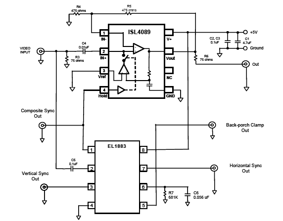
3 September 2008 I ordered more samples, this time from Intersil. If you look at this waveform, I'm going to have to DC restore the incoming video signal using a video clamping circuit like the ISL4089 from Intersil. Once the sync tips are clamped to 0V, I can set up a fixed slice level to extract a digital data stream from the analog video. I'm planning to use the following circuit as an input circuit for the PCM decoder unit ie. PAL video --> PCM
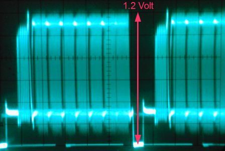
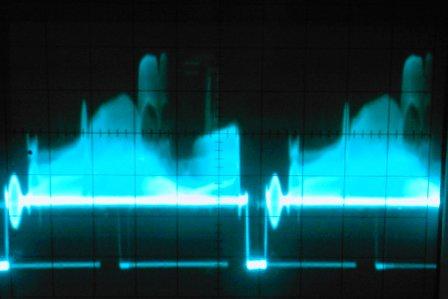
7 September 2008 It works! There are still some issues, but I'm getting a signal out which clearly corresponds with the PCM data. There is still some distortion in the video output. I think it is caused by the DCI interface interrupt causing some video pulses to be generated late. I'm going to set the DCI interrupt priority low as it only occurs every 11us with large gaps in-between giving the CPU plenty of time to service it.
Notice the wavy edge of the clock pulses in the video on the left. I lowered the priority of the DCI interrupt and that fixed the wobbly video timing. See the video on the right. The timing is now perfect. Samples are still being recorded in the sequence L0R0L1R1L2R2 or R0L1R1L2R2L3 etc. I have to ad interleaving and CRC. and the code as it appears now... 15 September 2008 Added code to calculate a checksum value for the data in each line and place the checksum at the end of the line. The checksum is a 16 bit signed integer calculated as follows: Sample1+Sample2+Sample3+Sample4+Sample5+Sample6=CHECKSUM The carry is ignored. The above value is written at the end of the line on the right of the screen. I also added code to ensure each line starts with a LEFT sample. This is done by splitting the single FIFO buffer into two. One for LEFT and one for RIGHT samples. The two FIFO buffers run in lock-step. When a sample is sitting in the DCI RXBUFF, a check is done on the COFS to see if the current sample is LEFT or RIGHT. The sample is then written into the corresponding FIFO. and the code as it appears now...
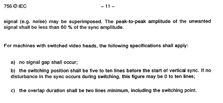
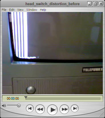
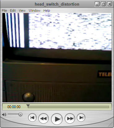
Samples are always recorded in the sequence L0R0L1R1L2R2 etc. I still have to ad interleaving. Notice the new checksum on the right 16 September 2008 It occurred to me today that I've never actually looked at the video output of the PCM-X2 encoder unit on an oscilloscope. The video output looks neat with all waveforms properly shaped. The video signal is 610mV peak-to-peak. I would like the output to be closer to 1Vp-p in the final version. This would only require tweaking the resistors in the 2-bit DAC. 20 September 2008 I made some test recordings of the data signal and noticed that the data signal is distorted due to the head switch that occurs on all VCRs. The head switch occurs 5- 10 lines before the vertical sync. Previously I inserted 18 blank lines at the beginning of every field, but I've now moved it to the end of the field. This means no data is recorded at the end of the field where the head switch occurs. I now have this blank bit where I can place non-critical data like the words "PCM-X2". Later, later...I've also got a bee in my bonnet about time codes. I've thought of placing linear timecode on the mono audio track of the video tape and supplementing it with vertical interval timecode. This means that the PCM adapter will be able to provide tape counter and track time/number features. Also later, but I'm thinking ahead. I also found some more bugs. I was only recording 287 lines of data per field instead of 294 lines of data. This would have caused FIFO buffer overruns. Here is a snippet from IEC standard 756 for domestic video recorders:
It looks like the 10 lines before vertical sync is best left clear.
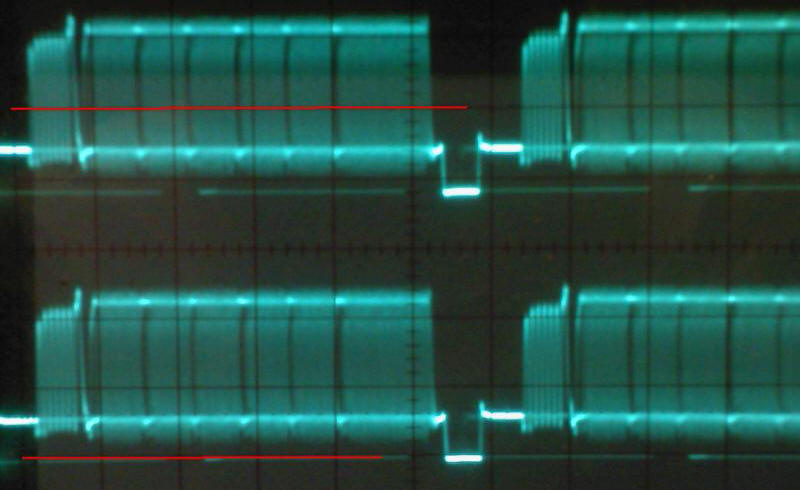
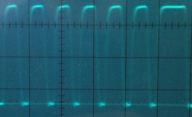
and the code as it appears now... 5 October 2008 I viewed the output of my VHS video recorder on the oscilloscope. Shown below is one line of video from the PCM-X2 encoder recorded onto VHS video tape. Once the sync tips are clamped to 0V, I'll be able to use one of the dsPIC33s onboard comparators to establish a fixed slice level to re-create a clean digital signal suitable for decoding. It may be possible, though not necessary, to have the dsPIC monitor the duty cycle of the extracted clock and adjust the slice level dynamically to obtain a 50% duty cycle. PCM-X2 encoder signal played back from VHS tape (below)
Recorded broadcast TV signal played back from VHS tape (below) Scale in both pictures is 0.2V/div
The input circuit to the PCM-X2 decoder board (below), will clamp the sync tips to 0V. Subsequent data slicing can then be performed by the dsPIC to extract data frames suitable for decoding. A data frame is equal to one line of video.
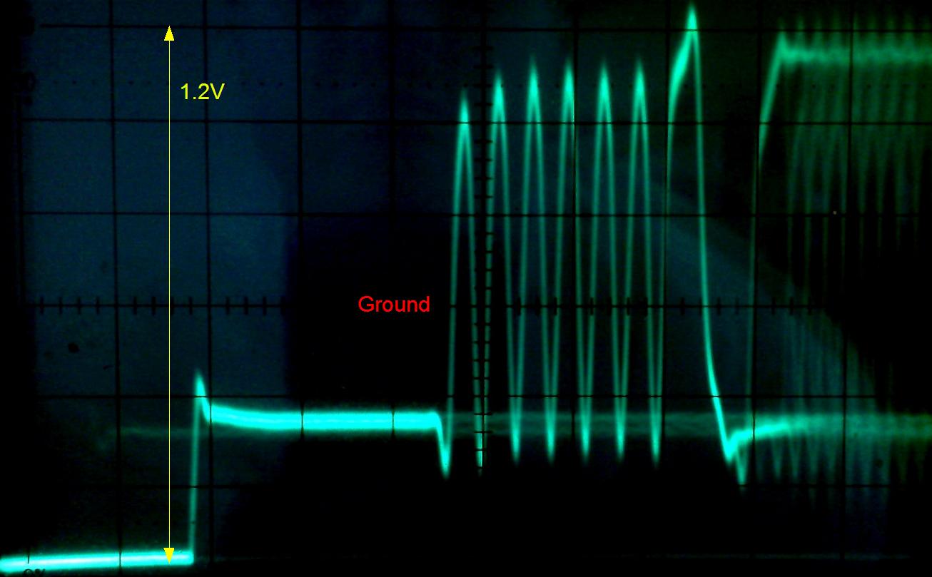
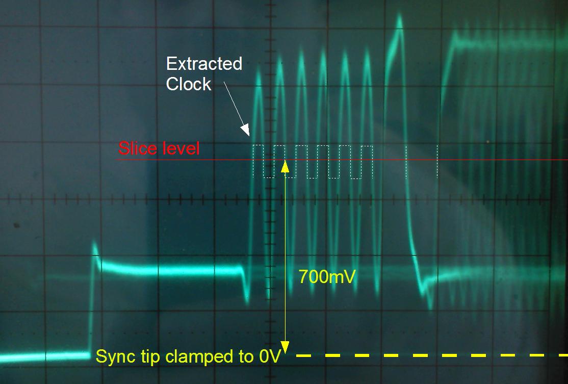
7 October 2008 I've been researching data slicers. Currently the video waveform swings around ground as shown below. This is due to the AC-coupling employed on the output of the VCR.
I plan to first clamp the sync tip to 0V and then to establish a slice level at 700mV as shown below. This should allow me to extract the clock and data as shown using a comparator. A diode can be used to provide the 0.7V reference.
9 October 2008 I'm just waiting for parts to start building the decoder unit. I've started thinking up some code for the decoding routine. The idea is that I'll use the line sync pulse to trigger an interrupt service routine to decode the incoming data frame. I'm not that keen to use the sync pulses. I'm not sure how reliable they are from a VCR. I'll try it first and see how it goes.... 14 October 2008 When I designed the PCMX2 encoder unit I was careful to make sure that the average data rate into my FIFO buffer is the same as the average data rate going out of my FIFO buffer. The code therefore does not contain any active FIFO management routines. It was assumed no buffer overruns would happen. In retrospect it is probably safer to add some kind of active FIFO buffer management routines. To avoid any surprises. To this end I'll be adding a mechanism whereby the reading out of samples can either be delayed by one video line, or an extra video line of data read out. Currently 294 lines of data is read out per field ie. 6 x 294 samples per field. I'll make it such that line 294 is left clear of data should the buffer start to get too empty. An extra line, 295, can be added to hold data should the buffer start getting too full. The ideal distance between the READ and WRITE pointers would be 1024 memory locations, but the distance will vary slightly during program execution. 15 October 2008 Added some FIFO management code. What the new code does is detect whether the distance between the read and write pointer is less than or greater than half the FIFO size. Based on this a decision is made on whether to output fewer samples or more samples. I'm not convinced its' working. I've added a trap to detect if the FIFO write and read pointers point to the same location. It's being triggered. All I can think is that the correction mechanism, adding or removing a line, only happens every 1/50s. This may not be fast enough to prevent an over-underrun. I'm going to change my strategy for reading out the data. 16 October 2008 Added code that keeps track of how many samples are available for unload in the FIFO buffer. I use a value called sample_count. Every time the write pointer is incremented, sample_count is incremented. Every time the read pointer is incremented, sample_count is decremented. Notice the main loop. If it should happen that the FIFO runs empty, the system halts ie for as long as there are samples available for unload, then proceed. main() and the code as it appears now... 19 October 2008 Began construction of the decoder unit.
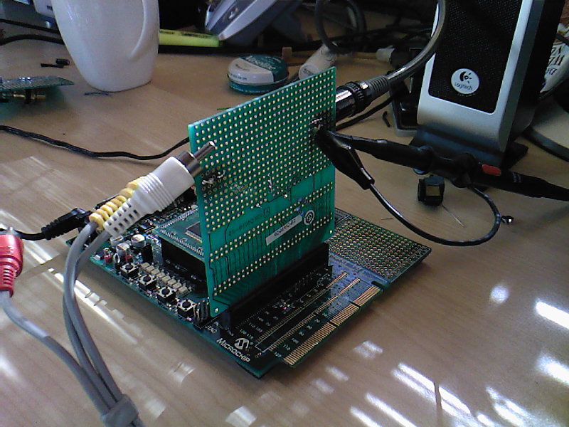
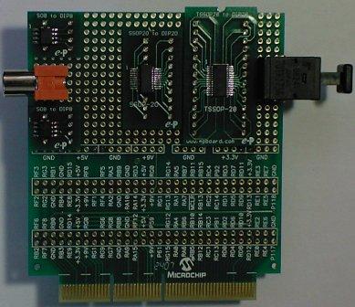
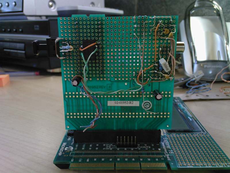
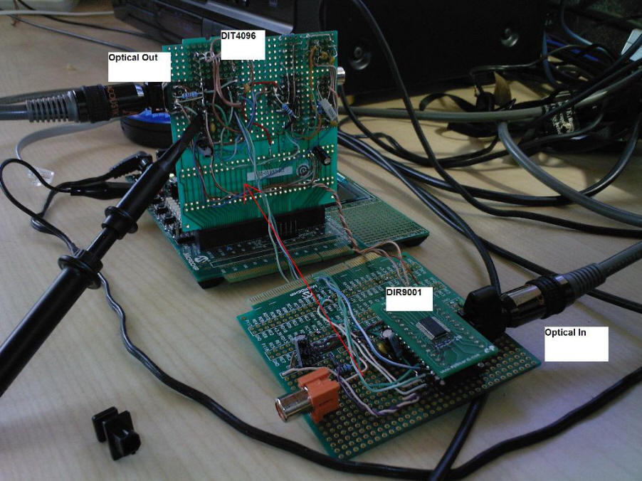
Baseband video input on the left, optical output to DAC on the right. The TOTX173 module is already installed. The adapter board next to it will take the DIT4096 SPDIF transmitter. 23 October 2008 With the bottom dropping out of the Rand, it just got more expensive to do my projects.<sigh> Watcha gonna do. Still waiting for adapter boards from epboard I ordered on 3/10. 1 November 2008 Got my adapter boards. Continuing the construction of the decoder card. I have to pick up some resistors, capacitors and a 27 MHz crystal on Monday.
4 November 2008 The analog front-end of the decoder card is working.
The top trace is the output of the VCR. Notice how the signal swings around ground (indicated by the red line). At the bottom is the output of the analog front-end. The sync tips have been clamped to 0V (indicated by the red line). Scale is 500mV/div
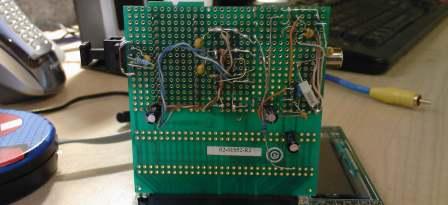
The decoder card is taking shape. 28 November 2008 Work on the decoder has stalled. I'm kept very busy with my day job. 1 December 2008 Tweaked some code in the encoder software. I added routines to capture FIFO buffer over-and- underruns. Also did some more construction on the decoder board. 2 December 2008 The PLL1705 clock generator is working. I salvaged the 27 MHz crystal from an old digital satellite receiver.
The decoder card as it looks now. The PLL1705 and its' 27MHz crystal is in the middle (top), the DIT4096, and the optical transmitter, is on the right
The front is much neater than the back. 3 December 2008 Removed the PLL1705 and replaced it with a CMX-309FL C, 11.2896 MHz clock generator IC. It has only four pins and require no external components. Much simpler. I mounted it underneath the DIT4096. The dsPIC33 will have to shuttle PCM samples to the DIT4096 for transmission over the optical fibre to an external DAC via the PICs Data Converter Interface. The DIT4096 should be able to provide the serial clock for the DCI, meaning the PIC can run at 80MHz or 40MIPS. I have to add a data slicer to the system to process the incoming analog video into a clean digital signal suitable for decoding. The dsPIC33 does have a built in comparator I could use, but I decided to use an external comparator for now. It would give me more control. I would like to add a feature, perhaps later, where the PIC monitors the duty cycle of the extracted clock signal. Using its' internal DAC it can then alter the reference voltage for the comparator so that an optimum slice point (50% clock duty cycle) is always achieved. This feature may negate the need for clamping the sync tips of the video signal to 0V as the PIC can alter the slice level dynamically.
Eye pattern of the data coming off the VHS tape. 0V is the solid line right at the bottom of the screen. Photographed at 200mV/div. Optimum data slicing point would be ~0.8V 5 & 6 December 2008 Did some major debugging again. In my previous code I had two FIFO buffers running in lock step to store L and R samples seperately. I discovered a bug where the WRITE pointer would skip alternate locations in the two FIFO buffers. I adjusted things back to a single buffer storing samples in LRLRLRLR configuration. When I did this the buffer overrun traps I set were being triggered. <sigh> Turns out the FIFO was experiencing buffer overruns for some reason. I tweaked the number of data lines (increase from 294 to 296 per field) read out until I got an underrun with all available data slots in all the lines filled. Then I added logic to delay the read-out of a some data lines until such time that the FIFO was half full. This had the effect of producing an up-down pulsing effect at the bottom of the screen as blank lines were read out to keep the buffer half full. <I tried to video it but it is almost impossible to see on the clip> So now the buffer over and underrun traps are NOT being triggered. Hooray! The blank lines are not a problem as I treat each video line as a data frame. If there is no header then there is no data. Finally I just want to say: " FIFO buffer management is a pain". I found that the most reliable way to monitor FIFO status is to monitor the actual number of samples available for read-out. I do this by incrementing a counter called sample_count every time I write a value to the FIFO and decrementing sample_count every time I read out a sample from the FIFO. This way if sample_count <= 0, then there was a buffer underrun. Also if sample_count > FIFO_SIZE, then there was a buffer overrun. I only read out samples if sample_count > (FIFO_SIZE/2) OR if I'm currently busy reading out a line. The last rule prevents half-full lines from being created. The system works perfectly with a FIFO with only 240 locations. That's 240 bytes! Current code 7 December 2008 The encoder was still producing partially filled data lines. I ran the code through MPLAB SIM and discovered the reason. If at the beginning of a line there wasn't enough samples in the buffer, the current line must not be filled with data at all. The program must wait 64us for the next line. This wasn't happening. Later in a line, data was still being entered. However, if you have started building a data line, you must finish it even if the FIFO is less than half full. I have to put the separate L and R sample buffers back. During debug I just read everything into the same buffer for simplicity. I hope, I pray, I trust that the FIFO is being run properly now. If I can get the decoder card and its' software working by 12/01/2009 it would be exactly one year since I started development of the PCM-X2.
Single field displayed, lines left empty to keep FIFO at half-full level Current code, stable and tested 8 December 2008 The data slicer using the LM319 is working. The incoming analog video is converted to a digital data stream. Next up, software.
The comparator with the trim-pot for the reference voltage.
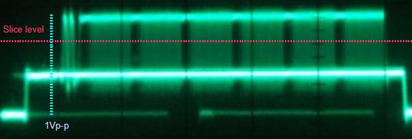
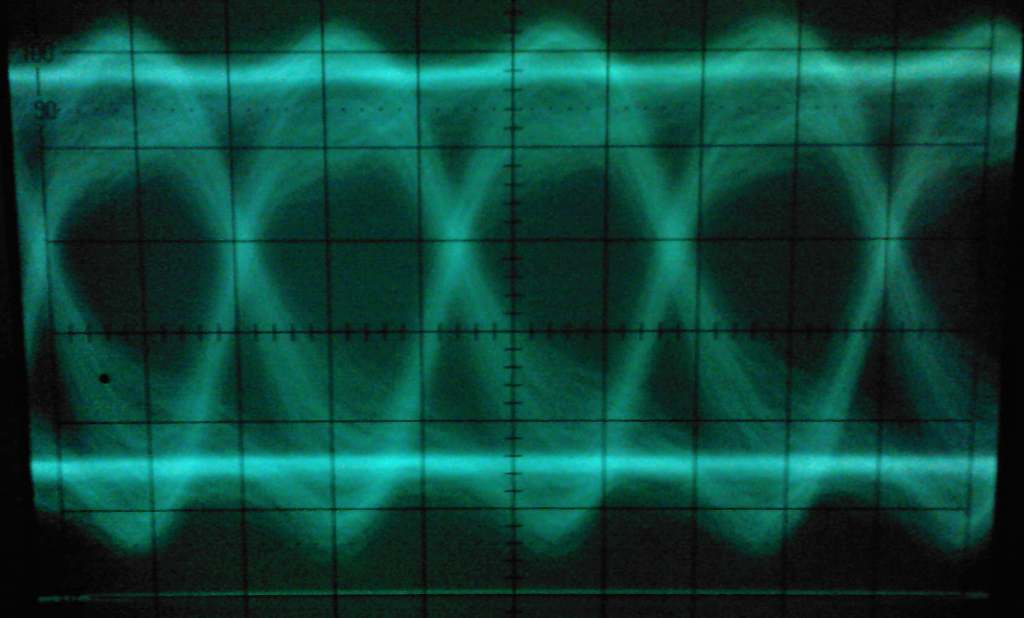
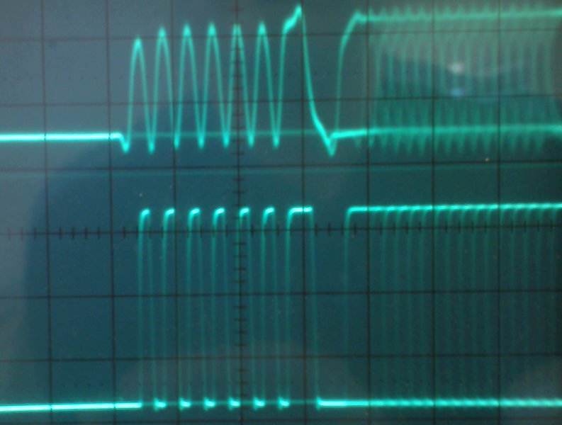
Input to the comparator is at the bottom @ ~1Vp-p, output from the comparator is at the top, 5Vp-p 10 December 2008 If you look at the picture above, the top trace has a slightly rounded shape. I'm not at all happy with this. The top trace is the output of the LM319 data slicer which uses a pull-up resistor on its' output. At the moment this pull-up is 3.3kOhm and I think it's affecting the rise time. I'm going to reduce the pull-up resistance to 1kOhm and see if the signal can get a more square shape.
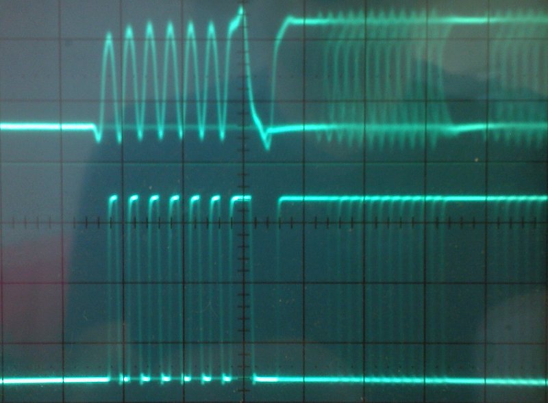
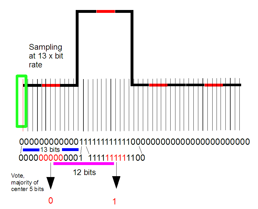
1K pull-up (above): Video signal (top), extracted data signal (bottom), clock run-in and first sample shown 680 ohm pull-up (below): Video signal (top), extracted data signal (bottom), clock run-in and first sample shown 13 December 2008 I'm researching ways of getting the data signal back into the dsPIC. I'm considering using a technique where I sample the input at an odd multiple of the data rate. I then store the samples in an array. I can then evaluate and decode the data frame after it has been received. The technique is based on a closed caption decoder found here.
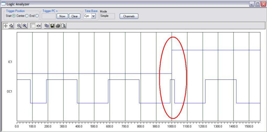
The first sample is synchronized with the first transition of the data signal. Samples are stored in an array. 13 bits at a time are read out and a vote is performed on the centre 5 bits. The majority is the decoded bit. I also thought of using the OC module and IC module to regenerate the clock signal and periodically resynching it with the clock from the data frame. I then use this clock to clock the data in via the SPI module. I did it! A PLL using a dsPIC33. Below is a free running clock (OC1). When a transition occurs on IC1, OC1 must sync itself to this edge. OC1 uses TMR3 as a timebase. Here's the code. Notice what happens inside the IC1 interrupt service routine. There is an 18 cycle latency between a transition on IC1 and OC1 resynching itself. At 40MIPS, 18 cycles is 450ns.
void _ISRFAST _IC1Interrupt( void) Digital PLL sample using dsPIC33
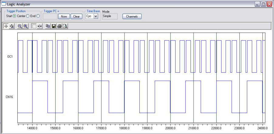
Another example uses the Change Notification module instead. In the picture below, notice how OC1 constantly realigns itself with the transitions in CN16. Latency is 16 cycles.
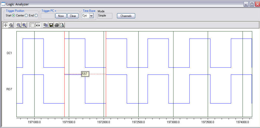
Code for example above I did some further experimentation using this code. Given an external and internal clock running at the same frequency and duty cycle, but NOT in phase, I can synchronize the dsPIC internal timebase with the external clock source within an accuracy of 325ns. The difference is due to latency in the dsPICs reactions to changes in the external clock. Given that the latency is known, it may be possible to program a correction factor into the TIMER3 value to compensate. I've adjusted the code again. Given two clocks running at the same frequency, but out of phase, one clock is external and the one is generated inside the dsPIC, I can now synchronise them perfectly.
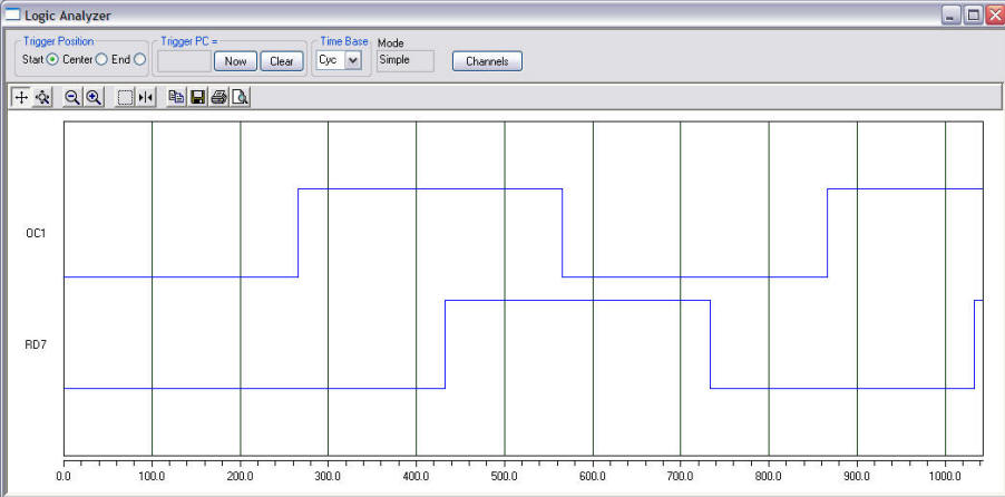
Internal timebase (OC1) and external timebase (RD7) out of phase [above] OC1 = RD7 = x Hz Perfectly in phase [below]
The code The dsPIC can periodically measure the frequency of the external timebase and readjust itself. 14 December 2008 ENCODER: It occurred to me that in a perfect world the audio samples coming in via the optical out of the CD player would arrive at exactly 88.2 kHz. This might not always be the case. I need to compensate for slight drifts in the output sample frequency of the audio source. At the moment, the video generating state machine in the dsPIC is driven by Timer3. Timer 3 uses the dsPICs own clock, ie 80MHz or 40MIPS. The DIR9001 has a SCKO output which provides a clock recovered from the incoming biphase data signal using a PLL. It runs at 512 x Fs or 22579200 Hz. I'd like to use this clock as the source for Timer 3 instead. This way, if the sampling rate of the audio source is slightly too high, the video lines will be generated slightly faster too. This means that the ratio of video lines-to-samples will be fixed. The variations should be minor and a VCR shouldn't have trouble locking on to a slightly fast or slow video signal. This may negate the need for an elaborate FIFO management system. I'm also going to start labelling my notes, so you know which unit I'm referring to. 15 December 2008 ENCODER: Experiments running Timer 3 off of SCKO from the DIR9001 did not produce satisfactory results. I've decided to keep generating video at 64μs/line, 50 fields/s and simply treating each video line as a data slot. Depending on the buffer level, slots can be filled or left open. In the decoder unit, a measure can be made of the number of samples arriving in one second. This will then set the playback sample rate. For example if during decoding, measurements show that stereo samples are arriving at 88203Hz, then that would be the playback rate. UPDATE 17/12/2008 I discovered why my attempt didn't work. According to this document, Timer 3 is a type C timer. This means that the input frequency is limited to half Fcy. Fcy in my project is 40MHz. This means the input clock must be less than half Fcy. I was feeding over 22MHz into Timer 3 which was much too high. 384 x Fs or 16934400 Hz would have been better. Fix for dsPIC that won't program or execute code I got extremely frustrated today. My dsPIC would not program. MPLAB would connect to the ICD2, I would program the chip but when I select "release from reset"....nothing. I knew the code was good because it worked before. I tried to load a demo program directly from Microchip, it also said it programmed, but it would not run. When this happens, try this:
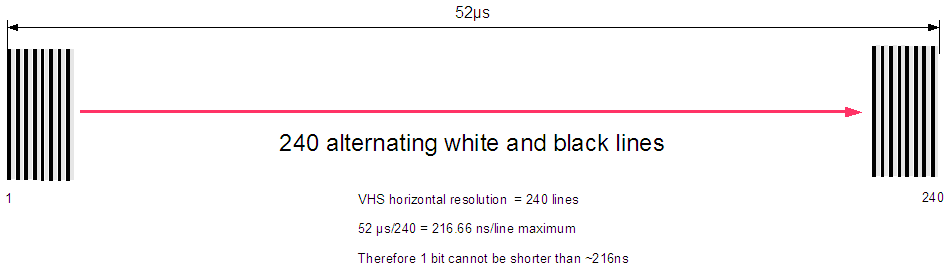
Try to load and execute your program now. I don't know why this works. I would sometimes get similar problems on PIC16F84s. ENCODER: I added code to calculate the incoming sampling rate. The calculated rate is written to a variable that I can then read using my in-circuit debugger. The sampling rate coming from my Sherwood CD player is 44103 Hz (0.0068 % off). This confirms my suspicion that samples are coming in slightly too fast. The stereo rate would be 88206 samples/second. Below is the current code: 17 December 2008 ENCODER: Currently each bit in my video output is ~400ns long. I currently have the following in one video line: Clock run-in (16bits) + 6 samples (6 * 16 bits) + 1 checksum (16 bits) total is 128 bits. If these 128 bits are set to alternating 1s and 0s, that's 128 horizontal lines in 52us.This equates to a video bandwidth of 1.641025 MHz. Here's how you work it out. My VCR seems to reproduce it just fine. Granted though that quite a bit of waveshaping has to be performed. So, up to 240 bits/line can be recorded. Could this open up the door for 18 bit/48kHz recording in later versions of my PCM encoder?
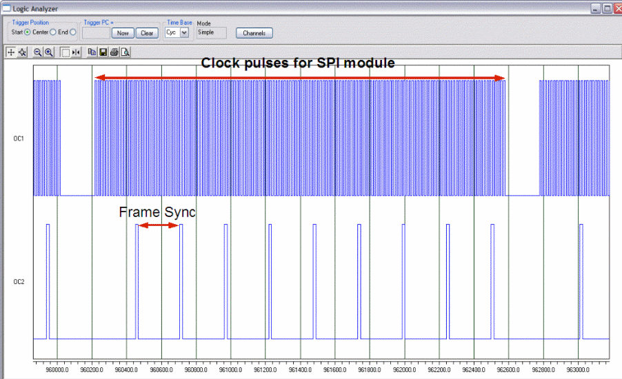
22 December 2008 Decoder: Wrote software to generate the clock pulses and frame sync pulses I'll need to shift the PCM data into the dsPIC via the SPI module. The clock pulse sequence just need to be aligned with the start of the data frame. This is accomplished by just switching the controlling timers on at the appropriate time. Below is the unload clock sequence for one video line. The frame sync pulses indicate to the SPI the word (sample) boundaries. There are more pulses than needed. Extra is just ignored once the correct number of samples are read in. I'm trying to use as many of the built-in peripherals as possible to reduce CPU overhead. Everything is happening very fast. I cannot use the Timer 3 or OC1 interrupts to do anything as they're way too short. I wasn't sure if I could get the combination of the frame sync and clock pulses to be produced properly. These documents helped though.
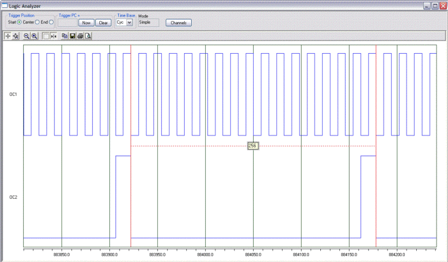
Below is one sample unload slot. 256 clock cycles wide. It contains 16 bit periods of 16 cycles each. The frame sync pulse indicate bit zero. OC1 polarity must be inverted still, but the timing is correct. Was tricky....
23 December 2008 Decoder: When sending samples out to the external DAC for playback, it is important that I match the rate at which samples are coming in from the VCR so as to avoid buffer over/underruns. To this end I'm planning on using a MAX9485 Programmable Audio Clock Generator. It's output frequency is tunable by ±200ppm. This will allow me to match the effective sampling rate of samples coming in from the VCR. I may also be able to use a Texas Instruments CDCE913. The decoder is proving more complex than I thought due to the need for wave shaping and clock regeneration. Did some more refining of the software so far. 25 December 2008 Decoder: Tested the DIT4096 and optical transmitter unit on the decoder board. I used the encoder unit to help me conduct the test. Look at the picture below, I fed the optical signal from the CD player into the DIR9001 on the encoder board. I then fed the binary data, L-R clock and serial clock from the DIR9001 to the DIT4096 to be retransmitted out via the optical transmitter. I need to make sure the peripherals work before I write the software.
27 December 2008 Working on the decoder board I discovered an error in the way the encoder encodes data. To make a long story short, the encoder was taking too long to load an SPI buffer during data line construction causing a timing problem. I fixed it now. Here's the latest code. 28 December 2008 The decoder board is generating the correct clock and frame-sync pulses. I can now feed the data signal from the VCR into the SPI interface on the dsPIC. I'll connect up the SPI bus and see if I can see the data in the receive buffer using the In-Circuit Debugger.
Above, data signal from tape (top) and the dsPIC generated SPI clock (below)
Things get kinda busy around Christmas
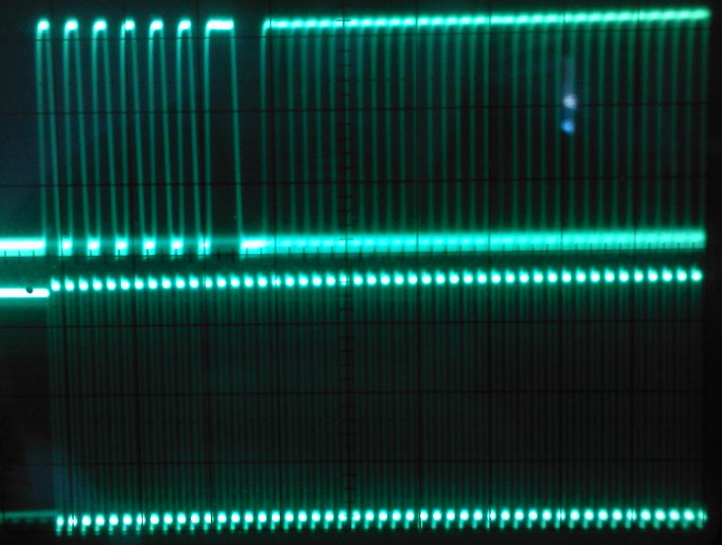
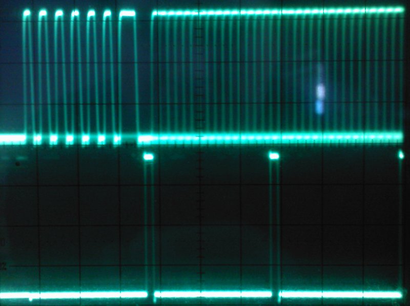
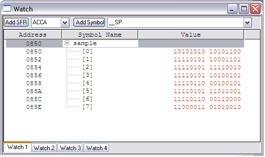
Above, data signal from tape (top) and the dsPIC generated frame sync (below). A high pulse is produced at bit 15 31 December 2008 After completely redesigning and reworking the SPI interface hardware and software, I have succeeded in reading in my first data frame from video tape. I could see the header and data in RAM and the checksum was correct. Below is data for ONE video line. Location [0] holds the clock run-in 10101010 10101100, locations [1] - [6] holds samples and location [7] holds the checksum. If you ad the data in locations [1] - [6] together you get 101 11000011 01010010 which matches [7]. Carries are ignored.
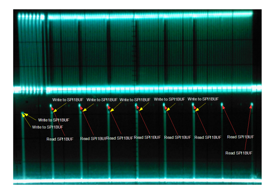
In the end of the day the SPI interface proved a real challenge, but I got it working. I'm operating the SPI interface in master mode. It generates it's own internal clock. All I had to do was make sure I write to the SPI1BUF at the correct time to start the transfer. I ONLY feed the data signal from the tape into the SPI. No external clock or frame sync was necessary. 2 January 2009 With the previous code I could only read one data frame before the SPI buffer would have an overflow [hey it was my first result]. I carefully debugged the problem. Data frames now flow in freely without causing overflows. The checksums also match. The code below fills an array with one data frame ready for processing. I think I got over a very hard part here. Just getting the samples back into the dsPIC from tape was quite a frustrating experience. I learnt a lot about how the SPI bus work though.
If you are new to SPI, please remember: For every write to the SPI1BUF there must be a corresponding read. In the picture above the relative read/write timing on the SPI bus for one data frame is shown. Notice how the sequence starts with two writes, followed by alternating read and writes. The sequence ends with two reads. Notice how there are 8 write and 8 read operations. The very first write operation is only there to activate the SPI clock. All subsequent writes are just dummy values to keep the SPI clock running (keep the transmit buffer full). 5 January 2009 First sound! I have managed to play back sound from the video tape. There is still some distortion due to bit errors. I'll have to track down the source. The data is definitely being read into the FIFO buffers correctly. Problems that still remain:
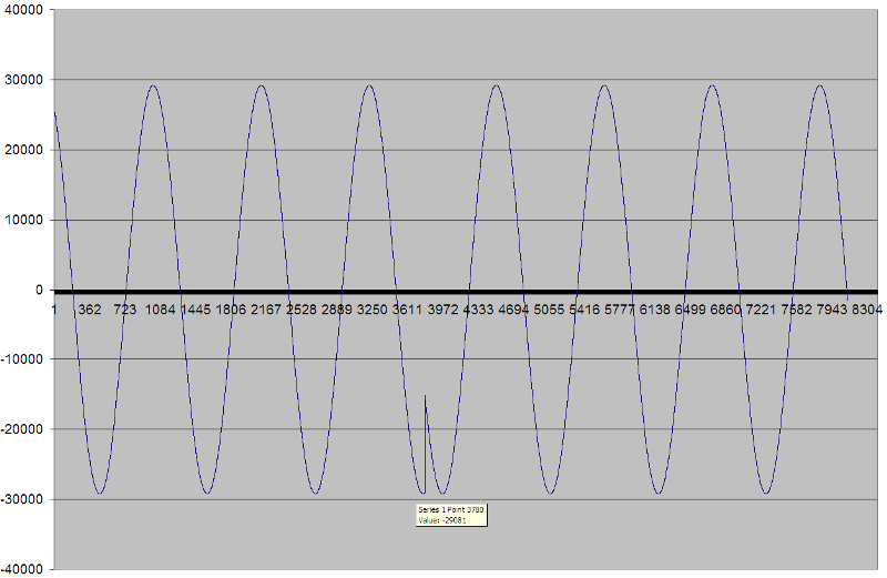
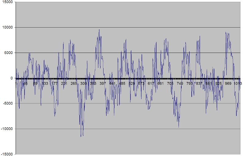
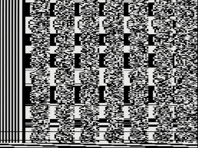
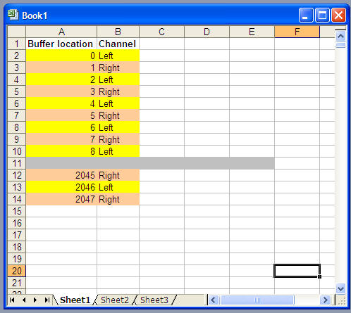
Building this system so far has taught me a lot about digital systems. I had to find solutions to several problems and revise my design as I went along. I've started analyzing the data path. I recorded some sample sine waves onto video tape using my encoder unit. I then played back the tape into the decoder and dumped the contents of the dsPIC RAM to EXCEL. Here's what the FIFO contents look like. The discontinuity in the middle is the location of the WRITE pointer. So old data is to the right and new data to the left. As you can see the sine wave is perfect. This means the encoder is working properly. The distortion during playback is due to the FIFO buffer issues. Old data is being played back. This issue should resolve itself once I can sync the playback rate to the rate at which the samples are played back from tape. In other words, the read pointer stays BEHIND the write pointer at all times without having to drop or repeat samples. I'm planning to use a MAX9485 VCXO (voltage controlled crystal oscillator) to generate the playback bit clock. It can be adjusted by ±200ppm which should be sufficient to allow the dsPIC to lock onto the rate at which samples arrive from tape.
FIFO buffer contents. Data as read from tape. Write pointer at 3780 7 January 2009 I discovered an interesting problem. I created a table of samples for a sine wave in Excel and stored the table in the dsPIC RAM. I then instructed the dsPIC to read out these samples as if it was reading out real samples from tape. With the video signal present on the input and data being read into the FIFO buffer the playback of the sine wave becomes choppy. It would seem the DCI is suffering from buffer underrun. As soon as the video signal is removed and the associated interrupt is no longer being triggered, the playback of the stored sine wave becomes perfect. I have been trying to avoid using DMA, but it looks like I have no choice. With the IC1 interrupt running the SPI and reading samples into RAM, the DCI can use DMA to read the samples out to the DAC without having to interrupt the IC1 process.
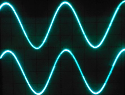
Managed to obtain distortion free playback of sine wave FROM TAPE. I tweaked the interrupt priorities. Still not using DMA.
Issues remaining:
Includes Excel spreadsheet analysis of FIFO RAM contents.
Snippet of music data in FIFO buffer [one channel], write pointer at 656 8 January 2009 Further analysis of FIFO buffer content did reveal periodic errors in the data frames being read in from tape. The cause appear to be jitter in the SPI clock caused by the DCI interrupt interrupting the SPI reads. Looks like I'm just going to have to make liberal use of DMA. I plan on using DMA to read data from tape into a frame buffer. Only when the frame buffer is full will it alert the CPU to copy the frame. While this is being done a new frame can be received. 9 January 2009 Code improved further. Data is now read out to DCI using DMA. Timing issues on SPI clock no longer present due to DCI using DMA. All data is read into and out of DMA RAM space, 1024 x 16 bits. Still have to add the VCXO to provide the proper playback clock.
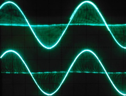
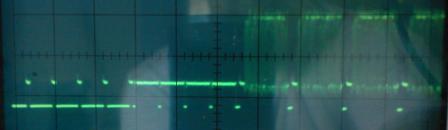
Left and Right channel output from DAC on oscilloscope
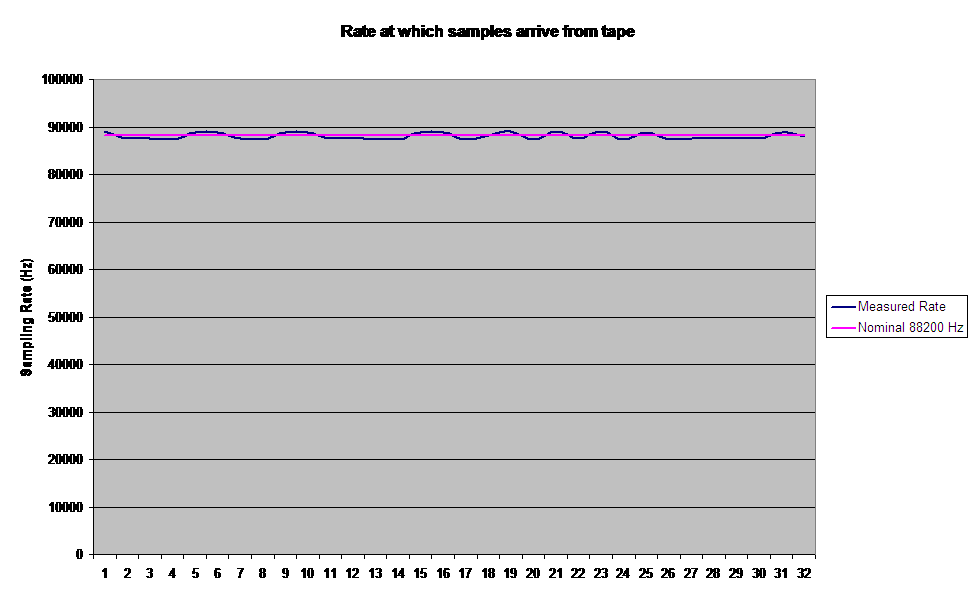
I measured the average rate at which samples arrive from tape. I'm pleased to say that it's within 0.16% of the expected rate of 88200Hz. Humans cannot hear a 0.16% pitch change.
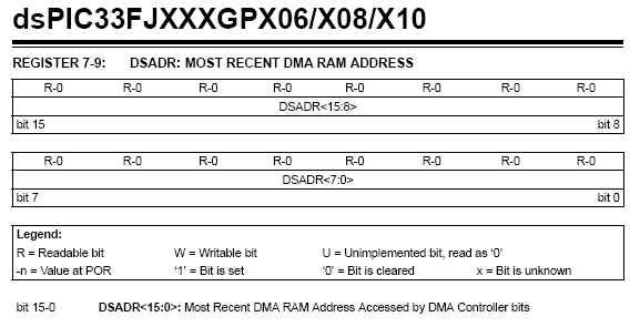
10 January 2009 Looking more closely at the DMA controllers' registers I found the "DSADR: MOST RECENT DMA RAM ADDRESS" register. This is perfect for keeping track of where the READ pointer is without constantly having to update a value manually. If I know where the READ pointer is, and I know where the WRITE pointer is, I can control the playback clock so that the READ pointer stays behind the WRITE pointer.
11 January 2009 Tired of looking at the DAC output on the oscilloscope, I captured a few seconds of tape playback to an MP3. The distortion is due to playback timing issues that still need fixing. I'm thinking of modifying the encoder unit slightly to include a few lines of the actual data clock, ie Fs x 64. This would be useful to sync to playback clock on the decoding end. 13 January 2009 My LG VCR died. SIGH! It won't display or record signals from its' AV input. Added circuits and code to the encoder unit to record a sample of the left-right (44100Hz) clock on some unused lines at the bottom of the frame. See bottom of picture below. In the future I would like to clock the dsPIC and DIR9001 from a single master clock. Then perhaps the lines at the bottom will be straight. I doesn't matter now.
Handed in the broken LG VCR at the store where I bought it for a warranty replacement. While I wait for them to assess my claim, I've bought an identical model in the meantime so I can continue my work. The model I bought is quite cheap, R575. I tested the new unit by recording some DSTV. It makes a remarkably clear and colourful picture for what it is. When I get the warranty replacement, I'll have a spare. New VHS VCRs are getting hard to find. Made a tape using the new code. Code now performs auto reset on system error, ie buffer under-overrun. 8 February 2009 I have the crystal and chip I need to finish the data clock for the PCM decoder. Just can't get to it now.... 22 May 2009 Tested the decoder board with code version 10012009a. Still OK. Encoder also OK. Haven't implemented the VCO yet. I may hold the VCO data clock over to version 3 of my PCM adapter. 13 February 2010 It occurred to me that I never checked to see if my VCR records the entire vertical blanking interval. Turns out it does and no data is being lost.
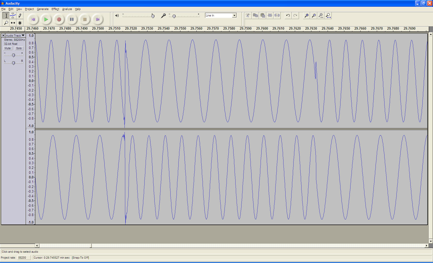
The PCM-X2 records data from line 6. From left to right are lines 1-5 in the EVEN field with data beginning on line 6 7 May 2010 Tested decoder with code version - 10012009a - OK Tested encoder with code version - 12012009 - OK The dsPIC33FJ256GP710 I'm using has 2048 bytes of DMA RAM where samples are stored. Playback analysis of a sine wave shows that anomalies occur every 1024 samples. The DMA RAM buffer is always kept half full of new samples. The other half contains old samples in the process of being overwritten. It is therefore possible to read out old content .
The analysis points, again, to the rate at which samples are loaded into the buffer and being taken out of the buffer not matching. The read pointer needs to stay behind the write pointer at all times. I believe this isn't happening. A PLL will be used in the PCM-X3 to lock onto the rate at which samples arrive from tape. By syncing the playback clock in this manner, the read pointer should stay behind the write pointer at all times. At the moment a free running playback clock is used. A beat is obviously occuring at the difference between the free running playback clock and the rate at which samples actually arrive. I also noticed that at each anomaly, L and R data get swapped over. There's more going on here than a timing problem...I'll have to do some more checking and testing. 8 May 2010
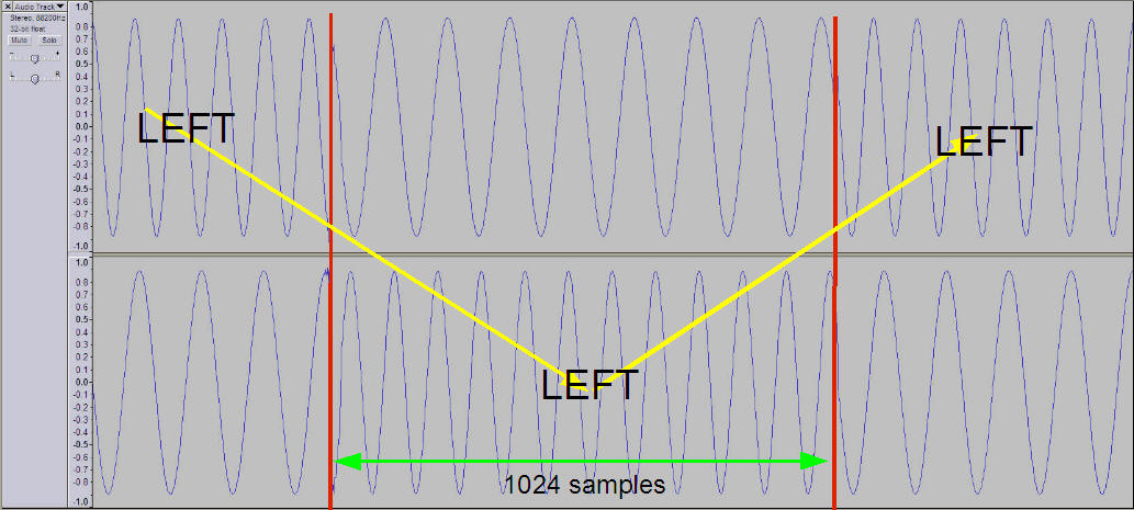
I think I know what's happening. The spreadsheet above shows how samples are spaced in DMA RAM. Odd locations store left samples and even locations store right samples. Somehow during the rollover of the read (or write) pointer from the end to the beginning of the buffer the read-out scheme gets swapped. Right samples are sent to the left channel and visa versa. An error in the calculation of the rollover can be occuring. As seen below reads for the left channel should always occur from odd numbered RAM locations, but instead it alternatively reads from odd locations and then even locations on successive passes. This results in the playback shown below. This is a buffer management and not a clock issue. I'll have to wait till I have time to analyze, confirm and fix the problem.
9 May 2010 Fixed the swapped channels and anomaly every 1024 samples. The problem was incorrect read out of DMA RAM due to an incorrect initialization of the DMA0CNT register. Playback is much clearer now. There are still the odd issue with channels being swapped around. I can fix this later by forcing certain samples to go to certain RAM/tape locations.
PCM-X2 playback test_TEST_TONES_09052010.mp3 PCM-X2 playback test_TEST_TONES_10012009a.mp3 16 May 2010 I've discovered another anomaly that repeats every 20ms or at a rate of 50Hz. Something is happening at the television field rate. I shall have to investigate. There is a gap in the data at the end of each field that lasts for ~18 lines. During this time it is possible that the read pointer momentarily overtakes the write pointer.
18 May 2010 Did more tests. I believe the buffer goes into underrun and then pulses between nearly full and empty at the field rate due to the data gap appearing every 20ms. This may be cured by the PLL to sync the playback clock to the rate at which samples arrive. Also, if the VCR is placed into CUE many invalid frames are created. These are skipped also resulting in buffer underrun. For the PCM-X3 the encoder unit will be synced to the sampling frequency. This will allow a fixed number of samples per video field. The decoder will then simply count lines and read in the appropriate number of data lines. No check will be performed (like now) to see if a video line has a valid header. I believe the two changes (PLL and sync to sampling rate) will alleviate or eliminate many of the errors that still occur in playback. I have deliberately not implemented error correction. I want playback as good as possible without it first, and then implement error correction. 18 January 2012 So nothing happened for a year. Too many other more important things happening. At least my Professor says my dissertation is "very close" to being finished. I'll hand in before middle of the year. Working on Goldilocks rekindled my desire to finish PCM-3 so I've been reflecting on clocks and such. The encoder will definitely use a clock which is a multiple of the sampling frequency fs. This means the encoder will produce a fixed number of audio samples per field. So fixed number of samples per second in, fixed number of samples per second out. DIR9001 will feed recovered data clock to dsPIC33. The issue I've been exploring is regeneration of the playback clock from the video signal at the decoder end. Like any good engineer I'd like to use the simplest solution possible and preferably as few additional chips as possible. The decoder dsPIC33 can perhaps be clocked from a crystal to run at 40MIPS, but it needs to be told how fast to send the samples to the DIT4096 so the buffers don't run empty.
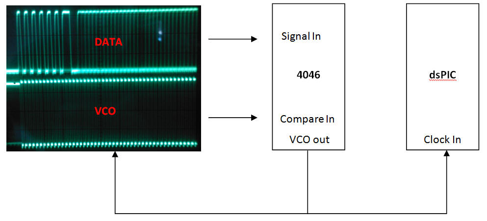
In the decoder the interrupt service routine (ISR) reading data in is triggered every time a new line starts by detecting the rising edge of the video sync pulse. The data stream on the left (top) can be sent directly to a 4046 phase with a VCO. It shouldn't matter that there's data on it. Since the encoder ran locked to fs the data stream will have a frequency component at a multiple of fs that the VCO can lock to. This will allow synchronisation of the local VCO to the playback clock. A type II Phase Comparator will be used. The resulting clock can then be used to clock the dsPIC33 and the DIT4096. Locking everything, including the PIC, to a single clock will allow the dsPIC SPI bus to dynamically follow minor changes in playback speed. The 4046 loop filter should remove jitter caused by the VHS transport. An LM565 can also be used or perhaps LMC568. FM demodulator chips seem to be of use here...
Recovering a master clock from input data stream. Centre frequency of 4046 is set by resistor/capacitor. 4046 Using phase comparator 2. 6 April 2012 I dismantled the prototype. There is NO WAY I'm using the 28 pin dsPIC33FJ128GP202. I'll make a new board. See Goldilocks for my reasons. I can't go any further with this hardware. On to the PCM-X3. |